
Specifications

dsPIC33F Family Reference Manual
DS70183A-page 16-4 © 2006 Microchip Technology Inc.
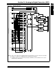
16.2 CONTROL REGISTERS
The ADC module has ten Control and Status registers. These registers are:
• ADxCON1: ADCx Control Register 1(1)
• ADxCON2: ADCx Control Register 2(1)
• ADxCON3: ADCx Control Register 3(1)
• ADxCON4: ADCx Control Register 4(1)
• ADxCHS123: ADCx Input Channel 1, 2, 3 Select Register(1)
• ADxCHS0: ADCx Input Channel 0 Select Register
• AD1CSSH: ADC1 Input Scan Select Register High
• ADxCSSL: ADCx Input Scan Select Register Low
• AD1PCFGH: ADC1 Port Configuration Register High
• ADxPCFGL: ADCx Port Configuration Register Low
The ADxCON1, ADxCON2 and ADxCON3 registers control the operation of the ADC module.
The ADxCON4 register sets up the number of conversion results stored in a DMA buffer for each
analog input in the Scatter/Gather mode. The ADxCHS123 and ADxCHS0 registers select the
input pins to be connected to the Sample/Hold amplifiers. The ADxPCFGH/L registers configure
the analog input pins as analog inputs or as digital I/O. The ADCSSH/L registers select inputs to
be sequentially scanned.