
Specifications


© 2006 Microchip Technology Inc. DS70183A-page 16-39
Section 16. Analog-to-Digital Converter (ADC)
A
D
C
16
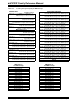
16.14.2 A/D Conversions While Scanning Through All Analog Inputs
Figure 16-18 and Table 16-3 illustrate a typical setup where all available analog input channels
are sampled by one Sample/Hold channel, CH0, and converted. The set Scan Input Selection
(CSCNA) bit (ADxCON2<10>) specifies scanning of the ADC inputs to the CH0 positive input.
Other conditions are similar to those described in Section 16.14.1 “Sampling and Converting
a Single Channel Multiple Times”.
Initially, the AN0 input is sampled by CH0 and converted. The result is stored in the user-config-
ured DMA buffer. Then the AN1 input is sampled and converted. This process of scanning the
inputs repeats 16 times until the buffer is full. Then the ADC module generates an interrupt. The
entire process then repeats.
Figure 16-18: Scanning Through 16 Inputs/Interrupt
ADC Clock
SAMP
Buffer[0]
TSAMP
TCONV
BSET AD1CON1,#ASAM
Instruction Execution
Buffer[1]
DONE
Buffer[2]
Buffer[15]
Input to CH0
AN0
TSAMP
TCONV
AN1
TSAMP
TCONV
AN14
TSAMP
TCONV
AN15
AD1IF
ASAM
Conversion
Trigger