
Specifications


© 2006 Microchip Technology Inc. DS70183A-page 16-33
Section 16. Analog-to-Digital Converter (ADC)
A
D
C
16
16.13 SPECIFYING CONVERSION RESULTS BUFFERING
The ADC module contains a single-word, read-only, dual-port register (ADCxBUF0), which
stores the A/D conversion result. If more than one conversion result needs to be buffered before
triggering an interrupt, DMA data transfers can be used. Both ADC channels (ADC1 and ADC2)
can trigger a DMA data transfer. Depending on which ADC channel is selected as the DMA IRQ
source, a DMA transfer occurs when the ADC Conversion Complete Interrupt Flag Status (AD1IF
or AD2IF) bit in the Interrupt Flag Status Register (IFS0 or IFS1, respectively) in the Interrupt
Module gets set as a result of a sample conversion sequence.
The result of every A/D conversion is stored in the ADCxBUF0 register. If a DMA channel is not
enabled for the ADC module, each result should be read by the user application before it gets
overwritten by the next conversion result. However, if DMA is enabled, multiple conversion
results can be automatically transferred from ADCxBUF0 to a user-defined buffer in the DMA
RAM area. Thus, the application can process several conversion results with minimal software
overhead.
The DMA Buffer Build Mode (ADDMABM) bit in ADCx Control Register 1 (ADxCON1<12>) deter-
mines how the conversion results are filled in the DMA RAM buffer area being used for the ADC.
If this bit is set (ADDMABM = 1), DMA buffers are written in the order of conversion. The ADC
module provides an address to the DMA channel that is the same as the address used for the
non-DMA stand-alone buffer. If the ADDMABM bit is cleared, then DMA buffers are written in
Scatter/Gather mode. The ADC module provides a Scatter/Gather address to the DMA channel,
based on the index of the analog input and the size of the DMA buffer.
16.13.1 USING DMA IN THE SCATTER/GATHER MODE
When the ADDMABM bit is ‘0’, the Scatter/Gather mode is enabled. In this mode, the DMA chan-
nel must be configured for Peripheral Indirect Addressing. The DMA buffer is divided into con-
secutive memory blocks corresponding to all available analog inputs (out of AN0 - AN31). Each
conversion result for a particular analog input is automatically transferred by the ADC module to
the corresponding block within the user-defined DMA buffer area. Successive samples for the
same analog input are stored in sequence within the block assigned to that input.
The number of samples that need to be stored in the DMA buffer for each analog input is speci-
fied by the DMABL<2:0> bits (ADxCON4<2:0>).
The buffer locations within each block are accessed by the ADC module using an internal pointer,
which is initialized to ‘0’ when the ADC module is enabled. When this internal pointer reaches
the value defined by the DMABL<2:0> bits, it gets reset to ‘0’. This ensures that conversion
results of one analog input do not corrupt the conversion results of other analog inputs. The rate
at which this internal pointer is incremented when data is written to the DMA buffer is specified
by the SMPI<3:0> bits.
When no channel scanning or alternate sampling is required, SMPI <3:0> should be cleared,
implying that the pointer will increment on every sample. Thus, it is theoretically possible to use
every location in the DMA buffer for the blocks assigned to the analog inputs being sampled.
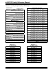
In the example illustrated in Figure 16-15, it can be observed that the conversion results for the
AN0, AN1 and AN2 inputs are stored in sequence, leaving no unused locations in their corre-
sponding memory blocks. However, for the four analog inputs (AN4, AN5, AN6 and AN7) that are
scanned by CH0, the first location in the AN5 block, the first two locations in the AN6 block and
the first three locations in the AN7 block are unused, resulting in a relatively inefficient arrange-
ment of data in the DMA buffer.
Note: For information about how to configure a DMA channel to transfer data from the
ADC buffer and define a corresponding DMA buffer area from where the data can
be accessed by the application, please refer to Section 22. “Direct Memory
Access (DMA)”. For specific information about the Interrupt registers, please refer
to Section 6. “Interrupts”.