
Specifications

© 2006 Microchip Technology Inc. DS70183A-page 16-3
Section 16. Analog-to-Digital Converter (ADC)
A
D
C
16
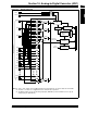
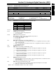
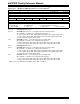
Figure 16-1: ADC Block Diagram
S/H
+
-
Conversion
Conversion Logic
VREF+
(1)
AVSS
AVDD
ADC
Data Format
16-bit
ADC Result
Bus Interface
00000
00101
00111
01001
11110
11111
00001
00010
00011
00100
00110
01000
01010
01011
AN30
AN31
AN8
AN9
AN10
AN11
AN2
AN4
AN7
AN0
AN3
AN1
AN5
CH1
(2)
CH2
(2)
CH3
(2)
CH0
AN5
AN2
AN11
AN8
VREF-
AN4
AN1
AN10
AN7
VREF-
AN3
AN0
AN9
AN6
VREF-
AN1
VREF-
VREF-
(1)
Sample/Sequence
Control
Sample
CH0,CH1,
CH2,CH3
Input MUX
Control
Input
Switches
S/H
+
-
S/H
+
-
S/H
+
-
AN6
Buffer
Result
Note 1: VREF+, VREF- inputs can be multiplexed with other analog inputs. See device data sheet for details.
2: Channels 1, 2 and 3 are not applicable for the 12-bit mode of operation.
3: The ADC1 module can use all 32 analog input pins (AN0-AN31), whereas ADC2 can use only 16
analog input pins (AN0-AN15).
Analog Input Pins
(3)