
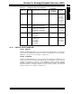
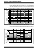
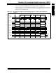
Specifications


© 2006 Microchip Technology Inc. DS70183A-page 16-27
Section 16. Analog-to-Digital Converter (ADC)
A
D
C
16
16.11.2.4 SAMPLE TIME CONSIDERATIONS USING CLOCKED CONVERSION
TRIGGER AND AUTOMATIC SAMPLING
Different sample/conversion sequences provide different available sampling times for the Sam-
ple/Hold channel to acquire the analog signal. The user must ensure the sampling time exceeds
the sampling requirements, as outlined in Section 16.15 “A/D Sampling Requirements”.
Assuming that the ADC module is set for automatic sampling and using a clocked conversion
trigger, the sampling interval is determined by the sample interval specified by the SAMC bits.
If the SIMSAM bit specifies simultaneous sampling or only one channel is active, the sampling
time is the period specified by the SAMC bit.
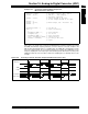
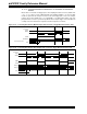
Equation 16-3: Available Sampling Time, Simultaneous Sampling
If the SIMSAM bit specifies sequential sampling, the total interval used to convert all channels is
the number of channels times the sampling time and conversion time. The sampling time for an
individual channel is the total interval minus the conversion time for that channel.
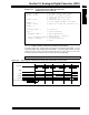
Equation 16-4: Available Sampling Time, Simultaneous Sampling
16.11.3 Event Trigger Conversion Start
It is often desirable to synchronize the end of sampling and the start of conversion with some
other time event. The ADC module can use one of three sources as a conversion trigger:
• External INT trigger
• GP Timer Compare trigger
• Motor Control PWM trigger
16.11.3.1 EXTERNAL INT TRIGGER
When SSRC<2:0> = 001, the A/D conversion is triggered by an active transition on the INT0 pin.
The INT0 pin can be programmed for either a rising edge input or a falling edge input.
16.11.3.2 GP TIMER COMPARE TRIGGER
The ADC is configured in this Trigger mode by setting SSRC<2:0> = 010. When a match occurs
between the 32-bit timer TMR3/TMR2 and the 32-bit Combined Period register PR3/PR2, a
special ADC trigger event signal is generated by Timer3. This feature does not exist for the
TMR5/TMR4 timer pair. Refer to Section 11. “Timers” for more details. Check for the most
recent documentation on the Microchip website at www.microchip.com.
16.11.3.3 MOTOR CONTROL PWM TRIGGER
The PWM Module has an event trigger that allows A/D conversions to be synchronized to the
PWM time base. When SSRC<2:0> = 011, the A/D sampling and conversion times occur at any
user programmable point within the PWM period. The special event trigger allows the user to
minimize the delay between the time when A/D conversion results are acquired and the time
when the duty cycle value is updated. Refer to Section 14. “Motor Control PWM” for more
details. Check for the most recent documentation on the Microchip website at
www.microchip.com.
T
SEQ = Channels per Sample (CH/S) *
((SAMC<4:0> * T
AD) + Conversion Time (TCONV))
T
SMP =(TSEQ – TCONV)
Note 1: CH/S specified by CHPS<1:0> bits.
2: TSEQ is the total time for the sample/convert sequence.
TSMP = SAMC<4:0> * TAD