
Specifications


dsPIC33F Family Reference Manual
DS70183A-page 16-18 © 2006 Microchip Technology Inc.
16.7 SELECTING ANALOG INPUTS FOR SAMPLING
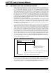
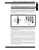
All Sample/Hold Amplifiers have analog multiplexers (see Figure 16-1) on both their non-invert-
ing and inverting inputs to select which analog input(s) are sampled. Once the sample/convert
sequence is specified, the ADxCHS0 and ADxCHS123 registers determine which analog inputs
are selected for each sample.
Additionally, the selected inputs can vary on an alternating sample basis or on a repeated
sequence of samples.
The same analog input can be connected to two or more Sample/Hold channels to improve con-
version rates.
16.7.1 Configuring Analog Port Pins
The ADPCFGH and ADPCFGL registers specify the input condition of device pins used as ana-
log inputs. Along with the Data Direction (TRISx) register in the Parallel I/O Port module, these
registers control the operation of the ADC pins.
A pin is configured as analog input when the corresponding PCFGn bit (ADPCFGH<n> or
ADPCFGL<n>) is clear. The ADPCFGH and ADPCFGL registers are clear at Reset, causing the
ADC input pins to be configured for analog input by default at Reset.
When configured for analog input, the associated port I/O digital input buffer is disabled so it does
not consume current.
The port pins that are desired as analog inputs must have their corresponding TRIS bit set, spec-
ifying port input. If the I/O pin associated with an A/D input is configured as an output, the TRIS
bit is cleared and the port’s digital output level (V
OH or VOL) is converted. After a device Reset,
all TRIS bits are set.
A pin is configured as digital I/O when the corresponding PCFGn bit is set. In this configuration,
the input to the analog multiplexer is connected to AVss.
16.7.2 Channel 0 Input Selection
Channel 0 is the most flexible of the four Sample/Hold channels in terms of selecting analog
inputs. It allows you to select any of the up to 16 analog inputs as the input to the positive input
of the channel. The Channel 0 Positive Input Select for Sample A (CH0SA<4:0>) bits
(ADxCHS0<4:0>) normally select the analog input for the positive input of channel 0.
You can select either V
REF- or AN1 as the negative input of the channel. The CH0NA bit
(ADxCHS0<7>) normally selects the analog input for the negative input of channel 0.
16.7.2.1 SPECIFYING ALTERNATING CHANNEL 0 INPUT SELECTIONS
The Alternate Input Sample Mode Select (ALTS) bit (ADxCON2<0>) causes the ADC module to
alternate between two sets of inputs that are selected during successive samples.
The inputs specified by CH0SA<4:0> (ADxCHS0<4:0>), CH0NA (ADxCHS0<7>), CH123SA
(ADxCHS123<0>) and CH123NA<1:0> (ADxCHS123<2:1>) are collectively called the MUX A
inputs. The inputs specified by CH0SB<4:0> (ADxCHS0<12:8>), CH0NB (ADxCHS0<15>),
CH123SB (ADxCHS0<8>) and CH123NB<1:0> (ADxCHS0<10:9>) are collectively called the
MUX B inputs. When the ALTS bit is ‘1’, the ADC module alternates between the MUX A inputs
on one group of samples and the MUX B inputs on the subsequent group of samples.
Note: Different devices will have different numbers of analog inputs. Verify the analog
input availability against the device data sheet.
Note 1: When the ADC Port register is read, any pin configured as an analog input reads
as a ‘0’.
2: Analog levels on any pin that is defined as a digital input (including the AN15:AN0
pins) may cause the input buffer to consume current that is out of the device’s
specification.