
Specifications


© 2006 Microchip Technology Inc. DS70183A-page 16-17
Section 16. Analog-to-Digital Converter (ADC)
A
D
C
16
16.6 SELECTING THE A/D CONVERSION CLOCK
The ADC module has a maximum rate at which conversions can be completed. An analog
module clock, T
AD, controls the conversion timing. The A/D conversion requires 12 clock periods
(12 T
AD) in the 10-bit mode and 14 clock periods (14 TAD) in the 12-bit mode. The A/D conversion
clock is derived from either the device instruction clock or an internal RC clock source.
The period of the A/D conversion clock is software selected using a 6-bit counter. There are 256
possible options for T
AD, specified by the ADC Conversion Clock Select (ADCS<7:0>) bits
(ADxCON3<7:0>). Equation 16-1 gives the T
AD value as a function of the ADCS control bits and
the device instruction cycle clock period, T
CY.
Equation 16-1: A/D Conversion Clock Period
For correct A/D conversions, the A/D conversion clock (T
AD) must be selected to ensure a
minimum T
AD time of 75 nsec.
The ADC module has a dedicated internal RC clock source that can be used to perform
conversions. The internal RC clock source should be used when A/D conversions are performed
while the device is in Sleep mode. The internal RC oscillator is selected by setting the ADC Con-
version Clock Source (ADRC) bit (ADxCON3<15>). When the ADRC bit is set, the ADCS<7:0>
bits have no effect on the A/D operation.
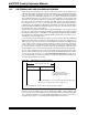
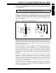
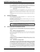
Figure 16-4: A/D Conversion Clock Period Block Diagram
T
AD = TCY(ADCS + 1)
ADCS =
T
AD
TCY
– 1
0
1
ADC Internal
RC Clock
Clock Multiplier
1, 2, 3, 4, 5,..., 256
ADxCON3<15>
TCY
TAD
8
ADxCON3<7:0>
A/D Conversion