
Specifications


dsPIC33F Family Reference Manual
DS70183A-page 16-14 © 2006 Microchip Technology Inc.
16.3 A/D TERMINOLOGY AND CONVERSION SEQUENCE
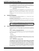
Figure 16-2 shows a basic conversion sequence and the terms that are used. A sampling of the
analog input pin voltage is performed by Sample/Hold amplifiers (also called Sample/Hold chan-
nels). The 10-bit ADC configuration can use up to four Sample/Hold channels, designated
CH0-CH3, whereas the 12-bit ADC configuration can use only one Sample/Hold channel, CH0.
The Sample/Hold channels are connected to the analog input pins via the analog input
multiplexer. The analog input multiplexer is controlled by the ADxCHS123 and ADxCHS0 regis-
ters. There are two sets of multiplexer control bits in the ADC channel select registers that func-
tion identically. These two sets of control bits allow two different analog input multiplexer
configurations to be programmed (called MUX A and MUX B). The ADC can optionally switch
between the MUX A and MUX B configurations between conversions. The ADC can also option-
ally scan through a series of analog inputs.
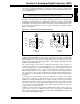
Sample time is the time that the ADC module’s Sample/Hold Amplifier is connected to the analog
input pin. The sample time can be started manually by setting the ADC Sample Enable (SAMP)
bit in ADCx Control Register 1 (ADxCON1<1>) or started automatically by the ADC hardware.
The sample time is ended manually by clearing the SAMP control bit in the user software or auto-
matically by a conversion trigger source.
Conversion time is the time required for the ADC to convert the voltage held by the Sample/Hold
Amplifier. The ADC is disconnected from the analog input pin at the end of the sample time. The
ADC requires one A/D clock cycle (T
AD) to convert each bit of the result plus two additional clock
cycles. A total of 12 T
AD cycles are required to perform the complete conversion in 10-bit mode.
A total of 14 T
AD cycles are required to perform the complete conversion in 12-bit mode. When
the conversion time is complete, the result is loaded into the ADCxBUF0 register, the Sam-
ple/Hold Amplifier can be reconnected to the input pin and a CPU interrupt can be generated.
The sum of the sample time and the A/D conversion time provides the total conversion time.
There is a minimum sample time to ensure that the Sample/Hold Amplifier provides the desired
accuracy for the A/D conversion (see 16.15 “A/D Sampling Requirements”). Furthermore,
there are multiple input clock options for the ADC. You must select an input clock option that does
not violate the minimum T
AD specification.
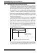
Figure 16-2: ADC Sample/Conversion Sequence
The ADC allows many options for specifying the sample/convert sequence. The sample/convert
sequence can be very simple, using only one Sample/Hold amplifier. A more elaborate sam-
ple/convert sequence performs multiple conversions using more than one Sample/Hold amplifier.
The 10-bit ADC configuration can use two Sample/Hold amplifiers to perform two conversions in
a sample/convert sequence or four Sample/Hold amplifiers with four conversions.
Sample Time
ADC Conversion Time
ADC Total Conversion Time
Sample/Hold Amplifier is connected to the analog input pin for sampling.
Sample/Hold Amplifier is disconnected from input and holds signal level.
A/D conversion is started by the conversion trigger source.
A/D conversion complete,
result is loaded into result buffer.
Optionally generate interrupt.