
Specifications


dsPIC33F Family Reference Manual
DS70183A-page 16-12 © 2006 Microchip Technology Inc.
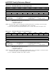
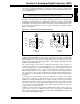
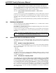
Register 16-7: AD1CSSH: ADC1 Input Scan Select Register High
R/W-0 R/W-0 R/W-0 R/W-0 R/W-0 R/W-0 R/W-0 R/W-0
CSS31 CSS30 CSS29 CSS28 CSS27 CSS26 CSS25 CSS24
bit 15 bit 8
R/W-0 R/W-0 R/W-0 R/W-0 R/W-0 R/W-0 R/W-0 R/W-0
CSS23 CSS22 CSS21 CSS20 CSS19 CSS18 CSS17 CSS16
bit 7 bit 0
Legend:
R = Readable bit W = Writable bit U = Unimplemented bit, read as ‘0’
-n = Value at POR ‘1’ = Bit is set ‘0’ = Bit is cleared x = Bit is unknown
bit 15-0 CSS<31:16>: ADC Input Scan Selection bits
(1, 2)
1 = Select ANx for input scan
0 = Skip ANx for input scan
Note 1: On devices with less than 32 analog inputs, all ADxCSSL bits can be selected by user. However, inputs
selected for scan without a corresponding input on device convert V
REF-.
2: ADC 2 only supports analog inputs AN0-AN15; therefore, no ADC 2 Input Scan Select register exists.
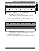
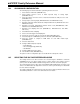
Register 16-8: ADxCSSL: ADCx Input Scan Select Register Low
R/W-0 R/W-0 R/W-0 R/W-0 R/W-0 R/W-0 R/W-0 R/W-0
CSS15 CSS14 CSS13 CSS12 CSS11 CSS10 CSS9 CSS8
bit 15 bit 8
R/W-0 R/W-0 R/W-0 R/W-0 R/W-0 R/W-0 R/W-0 R/W-0
CSS7 CSS6 CSS5 CSS4 CSS3 CSS2 CSS1 CSS0
bit 7 bit 0
Legend:
R = Readable bit W = Writable bit U = Unimplemented bit, read as ‘0’
-n = Value at POR ‘1’ = Bit is set ‘0’ = Bit is cleared x = Bit is unknown
bit 15-0 CSS<15:0>: ADC Input Scan Selection bits
(1, 2)
1 = Select ANx for input scan
0 = Skip ANx for input scan
Note 1: On devices with less than 16 analog inputs, all ADxCSSL bits can be selected by the user. However, inputs
selected for scan without a corresponding input on device convert V
REF-.
2: The ‘x’ in ADxCSSL and ADCx refers to ADC 1 or ADC 2.