
Specifications


© 2006 Microchip Technology Inc. DS70183A-page 16-11
Section 16. Analog-to-Digital Converter (ADC)
A
D
C
16
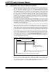
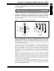
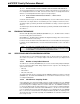
Register 16-6: ADxCHS0: ADCx Input Channel 0 Select Register
R/W-0 U-0 U-0 R/W-0 R/W-0 R/W-0 R/W-0 R/W-0
CH0NB
— — CH0SB<4:0>
bit 15 bit 8
R/W-0 U-0 U-0 R/W-0 R/W-0 R/W-0 R/W-0 R/W-0
CH0NA — — CH0SA<4:0>
bit 7 bit 0
Legend:
R = Readable bit W = Writable bit U = Unimplemented bit, read as ‘0’
-n = Value at POR ‘1’ = Bit is set ‘0’ = Bit is cleared x = Bit is unknown
bit 15 CH0NB: Channel 0 Negative Input Select for Sample B bit
Same definition as bit 7.
bit 14-13 Unimplemented: Read as ‘0’
bit 12-8 CH0SB<4:0>: Channel 0 Positive Input Select for Sample B bits
(1, 2)
Same definition as bit<4:0>.
bit 7 CH0NA: Channel 0 Negative Input Select for Sample A bit
1 = Channel 0 negative input is AN1
0 = Channel 0 negative input is V
REFL
bit 6-5 Unimplemented: Read as ‘0’
bit 4-0 CH0SA<4:0>: Channel 0 Positive Input Select for Sample A bits
(1, 2)
11111 = Channel 0 positive input is AN31
11110 = Channel 0 positive input is AN30
• • •
00010 = Channel 0 positive input is AN2
00001 = Channel 0 positive input is AN1
00000 = Channel 0 positive input is AN0
Note 1: The AN16 – AN31 pins are not available for ADC 2.
2: The ‘x’ in ADxCHS0 and ADCx refers to ADC 1 or ADC 2