6 HIGHLIGHTS This section of the manual contains the following major topics: 16.1 Introduction .................................................................................................................. 16-2 16.2 Control Registers ......................................................................................................... 16-4 16.3 A/D Terminology and Conversion Sequence ............................................................. 16-14 16.4 ADC Module Configuration ..................
dsPIC33F Family Reference Manual 16.1 INTRODUCTION The dsPIC33F family devices have up to 32 A/D input channels. These devices also have up to two ADC modules (ADCx, where x = 1 or 2), each with its own set of Special Function Registers (SFRs). The 10-bit or 12-bit Operation Mode (AD12B) bit in the ADCx Control 1(ADxCON1) register allows each of the ADC modules to be configured by the user application as either a 10-bit, 4 Sample/Hold (S/H) ADC (default configuration) or a 12-bit, 1 Sample/Hold ADC.
Section 16.
dsPIC33F Family Reference Manual 16.2 CONTROL REGISTERS The ADC module has ten Control and Status registers.
Section 16.
dsPIC33F Family Reference Manual Register 16-1: ADxCON1: ADCx Control Register 1(1) (Continued) bit 3 SIMSAM: Simultaneous Sample Select bit (only applicable when CHPS<1:0> = 01 or 1x) When AD12B = 1, SIMSAM is: U-0, Unimplemented, Read as ‘0’ 1 = Samples CH0, CH1, CH2, CH3 simultaneously (when CHPS<1:0> = 1x); or Samples CH0 and CH1 simultaneously (when CHPS<1:0> = 01) 0 = Samples multiple channels individually in sequence bit 2 ASAM: ADC Sample Auto-Start bit 1 = Sampling begins immediately after last
Section 16.
dsPIC33F Family Reference Manual Register 16-3: ADxCON3: ADCx Control Register 3(1) R/W-0 ADRC bit 15 R/W-0 U-0 — U-0 — R/W-0 R/W-0 R/W-0 SAMC<4:0> R/W-0 R/W-0 bit 8 R/W-0 R/W-0 R/W-0 R/W-0 ADCS<7:0> R/W-0 R/W-0 R/W-0 bit 7 Legend: R = Readable bit -n = Value at POR bit 0 W = Writable bit ‘1’ = Bit is set U = Unimplemented bit, read as ‘0’ ‘0’ = Bit is cleared x = Bit is unknown bit 15 ADRC: ADC Conversion Clock Source bit 1 = ADC Internal RC Clock 0 = Clock Derived From System Clock bi
Section 16.
dsPIC33F Family Reference Manual Register 16-5: ADxCHS123: ADCx Input Channel 1, 2, 3 Select Register(1) U-0 — bit 15 U-0 — U-0 — U-0 — U-0 — R/W-0 R/W-0 CH123NB<1:0> R/W-0 CH123SB bit 8 U-0 — U-0 — U-0 — U-0 — U-0 — R/W-0 R/W-0 CH123NA<1:0> R/W-0 CH123SA bit 0 bit 7 Legend: R = Readable bit -n = Value at POR W = Writable bit ‘1’ = Bit is set U = Unimplemented bit, read as ‘0’ ‘0’ = Bit is cleared x = Bit is unknown bit 15-11 bit 10-9 Unimplemented: Read as ‘0’ CH123NB<1:0>: Channel 1, 2
Section 16. Analog-to-Digital Converter (ADC) 16 Register 16-6: ADxCHS0: ADCx Input Channel 0 Select Register U-0 — R/W-0 CH0NA bit 7 U-0 — U-0 — R/W-0 R/W-0 R/W-0 CH0SB<4:0> R/W-0 R/W-0 bit 8 Legend: R = Readable bit -n = Value at POR U-0 — R/W-0 R/W-0 R/W-0 CH0SA<4:0> R/W-0 R/W-0 bit 0 W = Writable bit ‘1’ = Bit is set U = Unimplemented bit, read as ‘0’ ‘0’ = Bit is cleared x = Bit is unknown bit 15 CH0NB: Channel 0 Negative Input Select for Sample B bit Same definition as bit 7.
dsPIC33F Family Reference Manual Register 16-7: AD1CSSH: ADC1 Input Scan Select Register High R/W-0 CSS31 bit 15 R/W-0 CSS30 R/W-0 CSS29 R/W-0 CSS28 R/W-0 CSS27 R/W-0 CSS26 R/W-0 CSS25 R/W-0 CSS24 bit 8 R/W-0 CSS23 bit 7 R/W-0 CSS22 R/W-0 CSS21 R/W-0 CSS20 R/W-0 CSS19 R/W-0 CSS18 R/W-0 CSS17 R/W-0 CSS16 bit 0 Legend: R = Readable bit -n = Value at POR W = Writable bit ‘1’ = Bit is set U = Unimplemented bit, read as ‘0’ ‘0’ = Bit is cleared x = Bit is unknown CSS<31:16>: ADC Input Scan S
Section 16.
dsPIC33F Family Reference Manual 16.3 A/D TERMINOLOGY AND CONVERSION SEQUENCE Figure 16-2 shows a basic conversion sequence and the terms that are used. A sampling of the analog input pin voltage is performed by Sample/Hold amplifiers (also called Sample/Hold channels). The 10-bit ADC configuration can use up to four Sample/Hold channels, designated CH0-CH3, whereas the 12-bit ADC configuration can use only one Sample/Hold channel, CH0.
Section 16. Analog-to-Digital Converter (ADC) 16 The number of Sample/Hold amplifiers, or channels per sample, used in the sample/convert sequence is determined by the Channel Select (CHPS<1:0>) control bits in ADCx Control Register 2 (ADxCON2<9:8>). The 12-bit ADC configuration can only perform one conversion in a single sample/convert sequence. The CHPS bits are irrelevant in this case.
dsPIC33F Family Reference Manual 16.4 ADC MODULE CONFIGURATION The following steps should be followed for performing an A/D conversion: 1. 2. 3. 4. 5. 6. 7. 8. 9. 10. 11. 12. 13. 14. 15. 16.
Section 16. Analog-to-Digital Converter (ADC) 16 16.6 SELECTING THE A/D CONVERSION CLOCK The period of the A/D conversion clock is software selected using a 6-bit counter. There are 256 possible options for TAD, specified by the ADC Conversion Clock Select (ADCS<7:0>) bits (ADxCON3<7:0>). Equation 16-1 gives the TAD value as a function of the ADCS control bits and the device instruction cycle clock period, TCY.
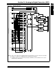
dsPIC33F Family Reference Manual 16.7 SELECTING ANALOG INPUTS FOR SAMPLING All Sample/Hold Amplifiers have analog multiplexers (see Figure 16-1) on both their non-inverting and inverting inputs to select which analog input(s) are sampled. Once the sample/convert sequence is specified, the ADxCHS0 and ADxCHS123 registers determine which analog inputs are selected for each sample. Additionally, the selected inputs can vary on an alternating sample basis or on a repeated sequence of samples.
Section 16. Analog-to-Digital Converter (ADC) 16 For channel 0, if the ALTS bit is ‘0’, only the inputs specified by CH0SA<4:0> and CH0NA are selected for sampling. Note that if multiple channels (CHPS = 01 or 1x) and simultaneous sampling (SIMSAM = 1) are specified, alternating inputs change every sample because all channels are sampled on every sample time.
dsPIC33F Family Reference Manual 16.7.3.1 SELECTING MULTIPLE CHANNELS FOR A SINGLE ANALOG INPUT The analog input multiplexer can be configured so that the same input pin is connected to two or more Sample/Hold channels. The ADC converts the value held on one Sample/Hold channel, while the second Sample/Hold channel acquires a new input sample. 16.7.3.
Section 16.
dsPIC33F Family Reference Manual 16.11 HOW TO STOP SAMPLING AND START CONVERSIONS The conversion trigger source terminates sampling and starts a selected sequence of conversions. The Sample Clock Source Select (SSRC<2:0>) bits (ADxCON1<7:5>) select the source of the conversion trigger. Note: The available conversion trigger sources can vary depending on the device variant. Please refer to the specific device data sheet for the available conversion trigger sources.
Section 16. Analog-to-Digital Converter (ADC) 16 Example 16-1: Converting 1 Channel, Manual Sample Start, Manual Conversion Start Code // // // // // AD1CHS0 = 0x0002; AD1CSSL = 0; AD1CON3 = 0x0002; AD1CON2 = 0; all PORTB = Digital; RB2 = analog SAMP bit = 0 ends sampling ... and starts converting Connect RB2/AN2 as CH0 input .. in this example RB2/AN2 is the input // Manual Sample, Tad = internal 2 Tcy AD1CON1bits.ADON = 1; // while (1) // { AD1CON1bits.SAMP = 1; // DelayNmSec(100); // AD1CON1bits.
dsPIC33F Family Reference Manual Example 16-2: Converting 1 Channel, Automatic Sample Start, Manual Conversion Start Code AD1PCFGL = 0xFF7F; AD1CON1 = 0x0004; AD1CHS0= 0x0007; AD1CSSL = 0; AD1CON3 = 0x0002; AD1CON2 = 0; // // // // // // all PORTB = Digital but RB7 = analog ASAM bit = 1 implies sampling .. starts immediately after last conversion is done Connect RB7/AN7 as CH0 input .. in this example RB7/AN7 is the input // Sample time manual, Tad = internal 2 Tcy AD1CON1bits.
Section 16. Analog-to-Digital Converter (ADC) 16 Example 16-3: Converting One Channel, Manual Sample Start, TAD Based Conversion Start Code AD1CHS0= 0x000C; AD1CSSL = 0; AD1CON3 = 0x1F02; AD1CON2 = 0; AD1CON1bits.ADON = 1; while (1) { AD1CON1bits.SAMP = 1; // // // // // // all PORTB = Digital; RB12 = analog SSRC bit = 111 implies internal counter ends sampling and starts converting. Connect RB12/AN12 as CH0 input ..
dsPIC33F Family Reference Manual 16.11.2.2 MULTIPLE CHANNELS WITH SIMULTANEOUS SAMPLING As shown in Figure 16-9 when using simultaneous sampling, the SAMC value specifies the sampling time. In the example, SAMC specifies a sample time of 3 TAD. Because automatic sample start is active, sampling starts on all channels after the last conversion ends and continues for three A/D clocks.
Section 16. Analog-to-Digital Converter (ADC) 16 16.11.2.4 SAMPLE TIME CONSIDERATIONS USING CLOCKED CONVERSION TRIGGER AND AUTOMATIC SAMPLING Assuming that the ADC module is set for automatic sampling and using a clocked conversion trigger, the sampling interval is determined by the sample interval specified by the SAMC bits. If the SIMSAM bit specifies simultaneous sampling or only one channel is active, the sampling time is the period specified by the SAMC bit.
dsPIC33F Family Reference Manual 16.11.3.4 SYNCHRONIZING A/D OPERATIONS TO INTERNAL OR EXTERNAL EVENTS Modes where an external event trigger pulse ends sampling and starts conversion (SSRC<2:0> = 001, 10, 011) can be used in combination with auto-sampling (ASAM = 1) to cause the ADC module to synchronize the sample conversion events to the trigger pulse source.
Section 16. Analog-to-Digital Converter (ADC) 16 16.11.3.5 MULTIPLE CHANNELS WITH SIMULTANEOUS SAMPLING Figure 16-13: Converting Four Channels, Auto-Sample Start, Trigger Conversion Start, Simultaneous Sampling TSEQ Conversion Trigger ADCLK TCONV TSAMP TCONV TCONV TCONV TSAMP ch0_samp ch1_samp ch2_samp ch3_samp Buffer[0] Buffer[1] Buffer[2] Buffer[3] DONE Cleared in software SAMP © 2006 Microchip Technology Inc.
dsPIC33F Family Reference Manual 16.11.3.6 MULTIPLE CHANNELS WITH SEQUENTIAL SAMPLING As shown in Figure 16-14 when sequential sampling is used, sampling for a particular channel stops just prior to converting that channel and resumes after the conversion has stopped.
Section 16. Analog-to-Digital Converter (ADC) 16 16.11.3.7 SAMPLE TIME CONSIDERATIONS FOR AUTOMATIC SAMPLING/CONVERSION SEQUENCES Assuming that the ADC module is set for automatic sampling and an external trigger pulse is used as the conversion trigger, the sampling interval is a portion of the trigger pulse interval. If the SIMSAM bit specifies simultaneous sampling, the sampling time is the trigger pulse period less the time required to complete the specified conversions.
dsPIC33F Family Reference Manual 16.12 CONTROLLING SAMPLE/CONVERSION OPERATION The application software can poll the SAMP (AD1CON1<1>) and DONE (AD1CON1<0>) bits to keep track of A/D operations or the ADC module can interrupt the CPU when conversions are complete. The application software can also abort A/D operations, if necessary. 16.12.1 Monitoring Sample/Conversion Status The SAMP and DONE bits indicate the sampling state and the conversion state of the ADC, respectively.
Section 16. Analog-to-Digital Converter (ADC) 16 16.13 SPECIFYING CONVERSION RESULTS BUFFERING The result of every A/D conversion is stored in the ADCxBUF0 register. If a DMA channel is not enabled for the ADC module, each result should be read by the user application before it gets overwritten by the next conversion result. However, if DMA is enabled, multiple conversion results can be automatically transferred from ADCxBUF0 to a user-defined buffer in the DMA RAM area.
dsPIC33F Family Reference Manual When scanning is used, and no simultaneous sampling is performed (SIMSAM = 0), SMPI<3:0> should be set to one less than the number of inputs being scanned. For example, if CHPS<1:0> = 00 (only one Sample/Hold channel is used), and AD1CSSL = 0xFFFF, indicating that AN0-AN15 are being scanned, then set SMPI<3:0> = 1111 so that the internal pointer is incremented only after every 16th sample/conversion sequence.
Section 16. Analog-to-Digital Converter (ADC) 16 Figure 16-15: DMA Buffer in Scatter/Gather Mode Unused Buffer Locations { Unused Buffer Locations { Unused Buffer Locations { Unused Buffer Locations { Unused Buffer Locations { Unused Buffer Locations { — — — — — — — © 2006 Microchip Technology Inc.
dsPIC33F Family Reference Manual 16.13.2 USING DMA IN THE CONVERSION ORDER MODE When the AADMABM bit (ADCON1<12>) = 1, the Conversion Order mode is enabled. In this mode, the DMA channel can be configured for Register Indirect or Peripheral Indirect Addressing. All conversion results are stored in the user-specified DMA buffer area in the same order in which the conversions are performed by the ADC module. In this mode, the buffer is not divided into blocks allocated to different analog inputs.
Section 16. Analog-to-Digital Converter (ADC) 16 16.14 CONVERSION SEQUENCE EXAMPLES 16.14.1 Sampling and Converting a Single Channel Multiple Times Figure 16-17 and Table 16-2 illustrate a basic configuration of the ADC. In this case, one ADC input, AN0, is sampled by one Sample/Hold channel, CH0, and converted. The results are stored in the user-configured DMA buffer, illustrated as Buffer(0) through Buffer(15).
dsPIC33F Family Reference Manual Table 16-2: Converting One Channel 16 Times per DMA Interrupt CONTROL BITS Sequence Select SMPI<3:0> = 0000, AMODE = 00, DMAxCNT = 15 DMA Interrupt on 16th conversion CHPS<1:0> = 00 Sample Channel CH0 SIMSAM = n/a Not applicable for single channel sample BUFM = 0 Single 16-word result buffer ALTS = 0 Always use MUX A input select MUX A Input Select CH0SA<4:0> = 00000 Select AN0 for CH0+ input CH0NA = 0 Select VREF- for CH0- input CSCNA = 0 No input scan CSSL<15:0> = n/a Sc
Section 16. Analog-to-Digital Converter (ADC) 16 16.14.2 A/D Conversions While Scanning Through All Analog Inputs Initially, the AN0 input is sampled by CH0 and converted. The result is stored in the user-configured DMA buffer. Then the AN1 input is sampled and converted. This process of scanning the inputs repeats 16 times until the buffer is full. Then the ADC module generates an interrupt. The entire process then repeats.
dsPIC33F Family Reference Manual Table 16-3: Scanning Through 16 Inputs per DMA Interrupt CONTROL BITS Sequence Select SMPI<3:0> = 1111, AMODE = 00, DMAxCNT = 15 DMA Interrupt on 16th conversion CHPS<1:0> = 00 Sample Channel CH0 SIMSAM = n/a Not applicable for single channel sample BUFM = 0 Single 16-word result buffer ALTS = 0 Always use MUX A input select MUX A Input Select CH0SA<4:0> = n/a Override by CSCNA CH0NA = 0 Select VREF- for CH0- input CSCNA = 1 Scan CH0+ Inputs CSSL<15:0> = 1111 1111 1111 111
Section 16. Analog-to-Digital Converter (ADC) 16 16.14.
dsPIC33F Family Reference Manual Table 16-4: Converting Three Inputs, Four Times and Four Inputs, One Time per DMA Interrupt CONTROL BITS Sequence Select SMPI<3:0> = 0011, AMODE = 00, DMAxCNT = 15 Scan 4 inputs, Interrupt on 16th conversion CHPS<1:0> = 1x Sample Channels CH0, CH1, CH2, CH3 SIMSAM = 1 Sample all channels simultaneously BUFM = 0 Single 16-word result buffer ALTS = 0 Always use MUX A input select MUX A Input Select CH0SA<3:0> = n/a Override by CSCNA CH0NA = 0 Select VREF- for CH0- input CSCN
Section 16. Analog-to-Digital Converter (ADC) 16 16.14.4 Using Alternating MUX A, MUX B Input Selections Note that using four Sample/Hold channels without alternating input selections results in the same number of conversions as this example, using two channels with alternating input selections. However, because the CH1, CH2 and CH3 channels are more limited in the selectivity of the analog inputs, this example method provides more flexibility of input selection than using four channels.
dsPIC33F Family Reference Manual Table 16-5: Converting Two Sets of Two Inputs Using Alternating Input Selections CONTROL BITS Sequence Select SMPI<3:0> = 0001, AMODE = 00, DMAxCNT = 7 Alt.
Section 16. Analog-to-Digital Converter (ADC) 16 16.14.5 Sampling Eight Inputs Using Simultaneous Sampling Figure 16-21 and Table 16-6 demonstrate simultaneous sampling. When converting more than one channel and selecting simultaneous sampling, the ADC module samples all channels, then performs the required conversions in sequence. In this example, with ASAM set, sampling begins after the conversions complete.
dsPIC33F Family Reference Manual Table 16-6: Sampling Eight Inputs Using Simultaneous Sampling CONTROL BITS Sequence Select SMPI<3:0> = 0001, AMODE = 00, DMAxCNT = 15 Alt.
Section 16. Analog-to-Digital Converter (ADC) 16 16.14.6 Sampling Eight Inputs Using Sequential Sampling When ASAM is clear, sampling does not resume after conversion completion but occurs when the SAMP bit is set. When utilizing more than one channel, sequential sampling provides more sampling time since a channel can be sampled while conversion occurs on another.
dsPIC33F Family Reference Manual Table 16-7: Sampling Eight Inputs Using Sequential Sampling CONTROL BITS Sequence Select SMPI<3:0> = 0001, AMODE = 00, DMAxCNT = 15 Alt.
Section 16. Analog-to-Digital Converter (ADC) 16 16.15 A/D SAMPLING REQUIREMENTS For the ADC module to meet its specified accuracy, the charge holding capacitor (CHOLD) must be allowed to fully charge to the voltage level on the analog input pin. The analog output source impedance (RS), the interconnect impedance (RIC) and the internal sampling switch (RSS) impedance combine to directly affect the time required to charge the capacitor CHOLD.
dsPIC33F Family Reference Manual 16.16 READING THE ADC RESULT BUFFER The RAM is 10-bits or 12-bits wide, but the data is automatically formatted to one of four selectable formats when the buffer is read. The FORM<1:0> bits (ADCON1<9:8>) select the format. The formatting hardware provides a 16-bit result on the data bus for all of the data formats. Figure 16-25 and Figure 16-26 show the data output formats that can be selected using the FORM<1:0> control bits.
Section 16.
dsPIC33F Family Reference Manual 16.17 TRANSFER FUNCTION (10-BIT MODE) The ideal transfer function of the ADC module is shown in Figure 16-27. The difference of the input voltages, (VINH – VINL), is compared to the reference, (VREFH – VREFL). • The first code transition (A) occurs when the input voltage is (VREFH – VREFL/2048) or 0.5 LSb. • The 00 0000 0001 code is centered at (VREFH – VREFL/1024) or 1.0 LSb (B). • The 10 0000 0000 code is centered at (512*(VREFH – VREFL)/1024) (C).
Section 16. Analog-to-Digital Converter (ADC) 16 16.18 TRANSFER FUNCTION (12-BIT MODE) • The first code transition (A) occurs when the input voltage is (VREFH – VREFL/8192) or 0.5 LSb. • The 00 0000 0001 code is centered at (VREFH – VREFL/4096) or 1.0 LSb (B). • The 10 0000 0000 code is centered at (2048*(VREFH – VREFL)/4096) (C). • An input voltage less than (1*(VREFH – VREFL)/8192) converts as 00 0000 0000 (D). • An input greater than (8192*(VREFH – VREFL)/8192) converts as 11 1111 1111 (E).
dsPIC33F Family Reference Manual 16.19 ADC ACCURACY/ERROR Refer to Section 16.26 “Related Application Notes” for a list of documents that discuss ADC accuracy. 16.20 CONNECTION CONSIDERATIONS Since the analog inputs employ ESD protection, they have diodes to VDD and VSS. As a result, the analog input must be between VDD and VSS. If the input voltage exceeds this range by greater than 0.
Section 16. Analog-to-Digital Converter (ADC) 16 Example 16-4: Code for Channel Scanning Using DMA #if defined(__dsPIC33F__) #include "p33fxxxx.h" #elif defined(__PIC24H__) #include "p24hxxxx.h" #endif void ProcessADCSamples(unsigned int * AdcBuffer); /*========================================================================================== ADC Initialization for Channel Scan ===========================================================================================*/ void initAdc1(void) { AD1CON1bits.
dsPIC33F Family Reference Manual Example 16-4: Code for Channel Scanning Using DMA (Continued) //AD1CHS123: A/D Input Select Register AD1CHS123bits.CH123SA = 0; // MUXA +ve input selection (AIN0) for CH1 AD1CHS123bits.CH123NA = 0; // MUXA -ve input selection (Vref-) for CH1 //AD1CSSH/AD1CSSL: A/D Input Scan Selection Register AD1CSSH = 0x0000; AD1CSSL = 0x000F; // Scan AIN0, AIN1, AIN2, AIN3 inputs AD1CON1bits.ADDMABM = 0; AD1CON2bits.SMPI = 3; AD1CON4bits.
Section 16. Analog-to-Digital Converter (ADC) 16 Example 16-4: Code for Channel Scanning Using DMA (Continued) // // // // // Configure DMA for Peripheral indirect mode Configure DMA for Continuous Ping-Pong mode Point DMA to ADC1BUF0 32 DMA request (4 buffers, each with 8 words) Select ADC1 as DMA Request source DMA0STA = __builtin_dmaoffset(&BufferA); DMA0STB = __builtin_dmaoffset(&BufferB); IFS0bits.DMA0IF = 0; IEC0bits.
dsPIC33F Family Reference Manual Example 16-5: Code for Alternate Sampling Using DMA /******************************************************************************************** * © 2005 Microchip Technology Inc. * * FileName: adcDrv1.c * Dependencies: Header (.h) files if applicable, see below * Processor: dsPIC33Fxxxx * Compiler: MPLAB® C30 v2.01.00 or higher * * SOFTWARE LICENSE AGREEMENT: * Microchip Technology Inc.
Section 16. Analog-to-Digital Converter (ADC) 16 Example 16-5: Code for Alternate Sampling Using DMA (Continued) // ADC Clock is derived from Systems Clock // ADC Conversion Clock Tad=Tcy*(ADCS+1)=(1/40M)*64 = 1.6us(625Khz) // ADC Conversion Time for 10-bit Tc=12*Tab = 19.2us AD1CON1bits.ADDMABM = 0; AD1CON2bits.SMPI = 1; AD1CON4bits.
dsPIC33F Family Reference Manual Example 16-5: Code for Alternate Sampling Using DMA (Continued) DMA0REQ=13; DMA0STA = __builtin_dmaoffset(&BufferA[0][0]); DMA0STB = __builtin_dmaoffset(&BufferB[0][0]); IFS0bits.DMA0IF = 0; IEC0bits.DMA0IE = 1; //Clear the DMA interrupt flag bit //Set the DMA interrupt enable bit DMA0CONbits.CHEN=1; } /*======================================================================================= _DMA0Interrupt(): ISR name is chosen from the device linker script.
Section 16. Analog-to-Digital Converter (ADC) 16 16.22 OPERATION DURING SLEEP AND IDLE MODES 16.22.1 CPU Sleep Mode without RC A/D Clock When the device enters Sleep mode, all clock sources to the ADC module are shut down and stay at logic ‘0’. If Sleep occurs in the middle of a conversion, the conversion is aborted unless the ADC is clocked from its internal RC clock generator. The converter does not resume a partially completed conversion on exiting from Sleep mode.
dsPIC33F Family Reference Manual 16.23 EFFECTS OF A RESET A device Reset forces all registers to their Reset state. This forces the ADC module to be turned off and any conversion in progress to be aborted. All pins that are multiplexed with analog inputs are configured as analog inputs. The corresponding TRIS bits are set. The value in the ADCxBUF0 register is not initialized during a Power-on Reset and contain unknown data. 16.
ADC Register Map File Name ADR Bit 15 Bit 14 Bit 13 Bit 12 Bit 11 Bit 10 Bit 9 Bit 8 Bit 7 Bit 6 Bit 5 Bit 4 Bit 3 INTCON1 0080 NSTDIS OVAERR OVBERR COVAERR COVBERR OVATE OVBTE COVTE SFTACERR DIV0ERR DMACERR MATHERR ADDRERR INTCON2 0082 ALTIVT DISI — — — — — — — — — INT4EP INT3EP INT2EP INT1EP INT0EP 0000 IFS0 0084 — DMA1IF AD1IF U1TXIF U1RXIF SPI1IF SPI1EIF T3IF T2IF OC2IF IC2IF DMA0IF T1IF OC1IF IC1IF INT0IF 0000 IFS1 0086 U2TXIF U2RX
dsPIC33F Family Reference Manual 16.25 DESIGN TIPS Question 1: How can I optimize the system performance of the ADC module? Answer: 1. 2. 3. Make sure you are meeting all of the timing specifications. If you are turning the ADC module off and on, there is a minimum delay you must wait before taking a sample. If you are changing input channels, there is a minimum delay you must wait for this as well. Finally, there is TAD, which is the time selected for each bit conversion.
Section 16. Analog-to-Digital Converter (ADC) 16 16.
dsPIC33F Family Reference Manual 16.27 REVISION HISTORY Revision A (December 2006) This is the initial release of this document. DS70183A-page 16-66 © 2006 Microchip Technology Inc.