
Specifications
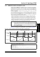


dsPIC33F/PIC24H Family Reference Manual
DS70323E-page 43-92 © 2008-2012 Microchip Technology Inc.
43.14 POWER-SAVING MODES
This section discusses the operation of the High-Speed PWM module in Sleep mode and Idle
mode.
43.14.1 High-Speed PWM Operation in Sleep Mode
When the device enters Sleep mode, the system clock is disabled. Since the clock for the PWM
time base is derived from the system clock source (T
CY), that clock is also disabled and all
enabled PWM output pins that are in effect prior to entering Sleep mode are frozen in the output
states. If the High-Speed PWM module is used to control load in a power application, the
High-Speed PWM module outputs must be placed into a safe state before executing the PWRSAV
instruction. Depending on the application, the load can begin to consume excessive current
when the PWM outputs are frozen in a particular output state. In such a case, the override
functionality can be used to drive the PWM output pins into the inactive state.
If the fault inputs are configured for the High-Speed PWM module, the fault input pins continue
to function normally when the device is in Sleep mode. If one of the fault pins is driven low while
the device is in Sleep mode, the PWM outputs are driven to the programmed fault states. The
fault input pins can also wake the CPU from Sleep mode. If the fault pin interrupt priority is greater
than the current CPU priority, program execution starts at the fault pin interrupt vector location
upon wake-up. Otherwise, execution continues from the next instruction following the PWRSAV
instruction.
43.14.2 High-Speed PWM Operation in Idle Mode
The PWM module consists of a PWM Time Base Stop in Idle Mode bit, PTSIDL (PTCON<13>).
ThE PTSIDL bit (PTCON<13>) determines whether the PWM module continues to operate or
stop when the device enters Idle mode. If PTSIDL = 0, the module continues to operate as
normal. If PTSIDL = 1, the module is shutdown and its internal clocks are stopped. The system
cannot access the Special Function Registers (SFRs) in this mode. This is the minimum power
mode for the module. Stopped Idle mode functions such as Sleep mode and fault pins are
asynchronously active. The control of the PWM pins revert back to the GPIO bits associated with
the PWM pins if the PWM module enters an Idle state.
It is recommended that the user-assigned application disable the PWM outputs prior to entering
Idle mode. If the PWM module is controlling a power conversion application, the action of putting
the device into Idle mode will cause any control loops to be disabled, and most applications are
likely to experience issues unless they are explicitly designed to operate in an open loop mode.
43.14.3 Low-Speed Mode
This mode suggests two methods to reduce power consumption:
1. The PWM clock prescaler, selected through the PCLKDIV<2:0> bits (PTCON2<2:0>) and
(STCON2<2:0>), configures the PWM module to operate at slower speeds to reduce
power consumption. The power reduction can be achieved with the loss of PWM
resolution.
2. The High-Resolution PWM Period Disable bit, HRPDIS (AUXCONx<15>) and the
High-Resolution PWM Duty Cycle Disable bit, HRDDIS (AUXCONx<14>) disable the cir-
cuitry associated with the high-resolution duty cycle and PWM period. If the HRDDIS bit
is set, the circuitry associated with the high-resolution duty cycle, phase offset and dead
time for the respective PWM generator is disabled. If the HRPDIS bit (AUXCONx<15>) is
set, the circuitry associated with the high-resolution PWM period for the respective PWM
generator is disabled. Many applications typically need either a high-resolution duty cycle
or phase offset (for fixed frequency operation), or a high-resolution PWM period for vari-
able frequency modes of operation (such as Resonant mode). Very few applications
require both high-resolution modes simultaneously. The ability to reduce operating current
is always an advantage. When the HRPDIS bit is set, the smallest unit of measure for the
PWM period is 8 ns. If the HRDDIS bit is set, the smallest unit of measure for the PWM
duty cycle, phase offset and dead time is 8 ns.
Note: For more information on power-saving modes, refer to Section 9. “Watchdog
Timer (WDT) and Power-Saving Modes” (DS70196).