
Specifications


dsPIC33F/PIC24H Family Reference Manual
DS70323E-page 43-86 © 2008-2012 Microchip Technology Inc.
43.11.5 PWM Pin Swapping
The SWAP PWMxH and PWMxL Pins bit, SWAP (IOCONx<1>), if set to ‘1’, enables the
user-assigned application to connect the PWMxH signal to the PWMxL pin and the PWMxL
signal to the PWMxH pin. If the SWAP bit (IOCONx<1>) is set to ‘0’, the PWM signals are
connected to their respective pins.
To perform the swapping function on the PWM cycle boundaries, the Output Override
Synchronization bit, OSYNC (IOCONx<0>), must be set. If the user-assigned application
changes the state of the SWAP bit (IOCONx<1>) when the module is operating and the OSYNC
bit (IOCONx<0>) is clear, the SWAP function attempts to execute in the middle of a PWM cycle
and the operation yields unpredictable results.
The SWAP function must be executed prior to the application of dead time. Dead time processing
is required since execution of switch function can enable the transistors in the user-assigned
application that are previously in disable state, possibly causing current shoot-through.
The SWAP feature is useful for the applications that support multiple switching topologies with a
single application circuit board. It also enables the user-assigned application to change the
transistor modulation scheme in response to changing conditions.
The SWAP function can be implemented by using either of the following methods:
• Dynamic Swapping: In the dynamic swapping, the state of the SWAP bit can be changed
dynamically based on the system response (for example, SMPS Power Control).
• Static Swapping: In static swapping, the SWAP bit is set during the start-up configuration
and remains unchanged during the program execution or on-the-fly (for example, Motor
Control).
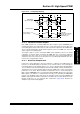
43.11.5.1 EXAMPLE 1: PIN SWAPPING WITH SMPS POWER CONTROL
The SMPS Power Control example describes dynamic swapping. In power conversion
applications, the transistor modulation technique can be changed between the full-bridge Zero
Voltage Transition (ZVT) and standard full-bridge “on-the-fly” transition to meet different load and
efficiency requirements. The generic full-bridge converter as illustrated in Figure 43-43, can
operate in Push-Pull mode. The transistors are configured as follows:
•Q1 = Q4
•Q2 = Q3
The generic full-bridge converter can also operate in ZVT mode. The transistors are configured
as follows:
•Q1 = PWM1H
•Q2 = PWM1L
•Q3 = PWM2H
•Q4 = PWM2L
Figure 43-43: SMPS Power Control
+
T1
V
OUT
+VIN
Q1
Q2
Q4
Q3