
Specifications


dsPIC33F/PIC24H Family Reference Manual
DS70323E-page 43-84 © 2008-2012 Microchip Technology Inc.
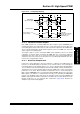
Figure 43-40: Dead-Time Compensation
43.11.4 Chop Mode
Many power control applications use transistor configurations that require an isolated transistor
gate drive. An example is a three-phase “H-bridge” configuration, where the upper transistors are
at an elevated electrical potential.
One method to achieve an isolated gate drive circuit is to use pulse transformers to couple the
PWM signals across a galvanic isolation barrier to the transistors. Unfortunately, in applications
that use either long duty cycle ratios, or slow PWM frequencies, the transformer’s low-frequency
response is poor. The pulse transformer cannot pass a long duration PWM signal to the isolated
transistor(s). If the PWM signals are “chopped” or gated by a high-frequency clock signal, the
high-frequency alternating signal easily passes through the pulse transformer. The chopping
frequency is typically hundreds or thousands of times higher in frequency as compared to the
PWM frequency. The higher the chopping (carrier) frequency relative to the PWM frequency, the
more the PWM duty cycle resolution is preserved.
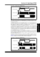
Figure 43-41 illustrates an example waveform of high-speed PWM chopping. In this example,
a 20 kHz PWM signal is chopped with a 500 kHz carrier generated by the chop clock.
Note: Dead-time compensation only applies to Complementary PWM Output mode.
Specifying dead-time compensation in any other PWM Output mode will yield
unpredictable results.
Normal PWM
Stretched PWM through DTR
Shortened PWM through DTR
DTCMPx selected PWMxH
Create PWMxL
PWMxH with ALDTR Dead Time
PWMxL with ALDTR Dead Time