
Specifications


© 2008-2012 Microchip Technology Inc. DS70323E-page 43-83
Section 43. High-Speed PWM
High-Speed PWM
43
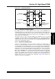
Figure 43-39: Leading-Edge Blanking
43.11.2 Individual Time Base Capture
Each PWM generator has a Primary PWM Time Base Capture register (PWMCAPx) that
automatically captures the independent time base counter value when the rising edge of the
current-limit signal is detected. This feature is active only after the application of the LEB function.
The user-assigned application should read the register before the next PWM cycle causes the
capture register to be updated again.
The Capture register is used in current-limit PWM control applications that use the analog
comparators or external circuitry to terminate the PWM duty cycle or period. By reading the
independent time base value at the current threshold, the user-assigned application can
calculate the slope of the current rise in the inductor. The secondary independent time base does
not have an associated Capture register.
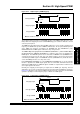
43.11.3 Dead-Time Compensation
In AC motor control applications, when the dead time is applied to the PWM signals, the
transistors are disabled. During the dead time, motor current continues to flow through the
recirculating diodes, but the applied voltage is zero. The zero applied voltage during dead time
causes a distortion of the desired voltage waveform and subsequently, a motor current distortion.
This distortion causes torque variations that can affect the stability of the control system and the
performance of the motor. When Dead-Time Compensation mode is selected through the
DTC<1:0> bits (PWMCONx<7:6>), an external input signal, DTCMPx, will cause the value in the
DTRx register to be added to, or subtracted from, the duty cycle specified by the MDC/PDCx
registers. The ALTDTRx register will specify the dead-time period for both the PWMxH and
PWMxL output signals. Dead-time compensation is available only for Positive Dead-Time mode.
Negative dead times are not supported with compensation. Figure 43-40 illustrates the
dead-time compensation timing diagram.
Switching Noise
Blanking time is determined by the
LEB<9:3> bits in the LEBCONx registers
Fault and current-limit
circuitry ignores the
switching noise
PWM Output
High Power Signal
Blanking Signal
Power signal as seen
by fault circuitry