
Specifications


dsPIC33F/PIC24H Family Reference Manual
DS70323E-page 43-6 © 2008-2012 Microchip Technology Inc.
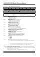
Register 43-1: PTCON: PWM Time Base Control Register
R/W-0 U-0 R/W-0 HS/HC-0 R/W-0 R/W-0 R/W-0 R/W-0
PTEN
(3)
— PTSIDL SESTAT SEIEN EIPU
(1)
SYNCPOL
(1,2)
SYNCOEN
(1,2)
bit 15 bit 8
R/W-0 R/W-0 R/W-0 R/W-0 R/W-0 R/W-0 R/W-0 R/W-0
SYNCEN
(1,2)
SYNCSRC<2:0>
(1,2)
SEVTPS<3:0>
(1)
bit 7 bit 0
Legend: HC = Cleared in Hardware HS = Set in Hardware
R = Readable bit W = Writable bit U = Unimplemented bit, read as ‘0’
-n = Value at POR ‘1’ = Bit is set ‘0’ = Bit is cleared x = Bit is unknown
bit 15 PTEN: PWM Module Enable bit
(3)
1 = PWM module is enabled
0 = PWM module is disabled
bit 14 Unimplemented: Read as ‘0’
bit 13 PTSIDL: PWM Time Base Stop in Idle Mode bit
1 = PWM time base halts in CPU Idle mode
0 = PWM time base runs in CPU Idle mode
bit 12 SESTAT: Special Event Interrupt Status bit
1 = Special Event Interrupt is pending
0 = Special Event Interrupt is not pending
bit 11 SEIEN: Special Event Interrupt Enable bit
1 = Special Event Interrupt is enabled
0 = Special Event Interrupt is disabled
bit 10 EIPU: Enable Immediate Period Updates bit
(1)
1 = Active Period register is updated immediately
0 = Active Period register updates occur on PWM cycle boundaries
bit 9 SYNCPOL: Synchronize Input and Output Polarity bit
(1,2)
1 = SYNCIx/SYNCO polarity is inverted (active-low)
0 = SYNCIx/SYNCO is active-high
bit 8 SYNCOEN: Primary Time Base Sync Enable bit
(1,2)
1 = SYNCO output is enabled
0 = SYNCO output is disabled
bit 7 SYNCEN: External Time Base Synchronization Enable bit
(1,2)
1 = External synchronization of primary time base is enabled
0 = External synchronization of primary time base is disabled
bit 6-4 SYNCSRC<2:0>: Synchronous Source Selection bits
(1)
011 = SYNCI4
010 = SYNCI3
001 = SYNCI2
000 = SYNCI1
bit 3-0 SEVTPS<3:0>: PWM Special Event Trigger Output Postscaler Select bits
(1)
1111 = 1:16 Postscaler generates Special Event Trigger on every sixteenth compare match event
•
•
•
0001 = 1:2 Postscaler generates Special Event Trigger on every second compare match event
0000 = 1:1 Postscaler generates Special Event Trigger on every compare match event
Note 1: These bits should be changed only when PTEN = 0.
2: The PWM Time base synchronization must only be used in the master time base with no phase shifting.
3: When the PWM module is enabled by setting PTCON<15> = 1, a delay will be observed before the PWM
outputs start switching. This delay is equal to:
PWM Turn ON delay = (2/ACLK) + (3 • (PCLKDIV setting)/ACLK) + 15 ns