
Specifications


dsPIC33F/PIC24H Family Reference Manual
DS70323E-page 43-54 © 2008-2012 Microchip Technology Inc.
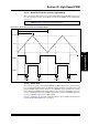
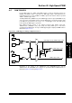
Figure 43-16: Phase Shifting (Complementary Mode)
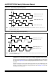
Figure 43-17: Phase Shifting (Independent Output Mode)
In addition, there are two shadow registers for the PHASEx and SPHASEx registers that are
updated whenever new values are written by the user-assigned application. These values are
transferred from the shadow registers to the PHASEx and SPHASEx registers on a Master time
base Reset. The actual application of these phase offsets on the PWM output occur on a master
time base Reset. Figure 43-18 provides the timing diagram that illustrates how these events are
generated.
The phase offset value can be any value between zero and the value in the PTPER register. Any
PHASEx or SPHASEx value greater than the PERIOD value is treated as a value equal to the
Period. It is not possible to create phase shifts greater than the Period. Example 43-17 provides
the PWM phase shift initialization.
PWMxH without Phase Shift
PWMxH with Phase Shift
PWMxL without Phase Shift
PWMxL with Phase Shift
PHASEx
Note: In Complementary, Push-Pull and Redundant PWM Output modes, PHASEx controls the phase shift for
PWMxH and PWMxL outputs.
PWMxH without Phase Shift
PWMxH with Phase Shift
PWMxL without Phase Shift
PWMxL with Phase Shift
Note: In Independent Output mode, SPHASEx controls the phase shift for PWMxL output, and PHASEx controls the
phase shift for PWMxH output.
(different duty cycle)
PHASEx
SPHASEx