
Specifications


dsPIC33F/PIC24H Family Reference Manual
DS70323E-page 43-48 © 2008-2012 Microchip Technology Inc.
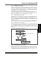
Figure 43-13: Secondary Duty Cycle Comparison
The Duty Cycle can be determined using Equation 43-5.
Equation 43-5: MDC, PDCx and SDCx Calculation
SDCx Register
STMRx
Compare Logic
PWMxL signal
0
15
15
MUX
MDC Register
MDCS select
01
CLK
15
0
0
<=
Note: In Independent Output mode, SDCx affects PWMxL only, SDCx is ignored in all other PWM
output modes.
MDC PDCx SDCx,,
ACLK 8× DesiredPWMDutyCycle×
PWMInputClockPrescalerDivider PCLKDIV()
----------------------------------------------------------------------------------------------------------------------------
⎝⎠
⎛⎞
=
ACLK
REFCLK M1×
N
--------------------------------------=
ACLK
7.49MHz 16×
1
----------------------------------- 119.84MHz==
(or)
Refer to Equation 43-1
ACLK
F
VCO
N
-------------=
Refer to Equation 43-2
Where,
REFCLK = 7.49 MHz
M1 = 16
N = 1
MDC PDCx SDCx,,
119.84MHz 8× 5μs×
1
------------------------------------------------------
⎝⎠
⎛⎞
4794==
Where,
The maximum PWM Duty Cycle resolution is 1.04 ns.
Desired PWM Duty Cycle = 5 µs
Note: The FRC clock can be tuned using the TUN<5:0> bits of OSCTUN special
function register to obtain a maximum PWM resolution of 1.04 ns. For further information
refer to the section on “Oscillator Configuration” in the device data sheet.
Note 1: If a duty cycle value is smaller than the minimum value (0x0008), a signal will have
zero duty cycle. A value of 0x0008 is the minimum usable duty cycle value that
produces an output pulse from the PWM generators.
2: A duty cycle value greater than (Period + 0x0008) produces 100% duty cycle.
3: If a duty cycle value is greater than or equal to the period value, a signal will have
a duty cycle of 100%.