
Specifications


© 2008-2012 Microchip Technology Inc. DS70323E-page 43-37
Section 43. High-Speed PWM
High-Speed PWM
43
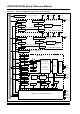
The ACLK for the PWM module can be derived from the system clock while the device is running
in the primary PLL mode. Equation 43-3 provides the relationship between the F
VCO frequency
and ACLK frequency. The block diagram for FVCO as the clock source for ACLK is illustrated in
Figure 43-4. The formula to calculate Fvco is shown in Equation 43-2. The example for using
F
VCO as the auxiliary clock source is shown in Example 43-3.
Figure 43-4: F
VCO is the Clock Source for Auxiliary Clock
Equation 43-2: FVCO Calculation
Equation 43-3: ACLK Frequency Calculation using F
VCO
0.8 MHz - 8.0 MHz
Here
(1)
112 MHz -120 MHz
Here
(1)
Divide by
2, 4, 8
Divide by
2-513
Divide by
2-33
Source (Crystal, External
PLLPRE
X
VCO
PLLDIV
PLLPOST
Clock or Internal RC)
12.5 MHz - 60 MHz
Here
(1)
FOSC
FVCO
N1
M
N2
Note 1: This frequency range must be satisfied when using F
VCO as the clock source for Auxiliary Clock.
FIN
F
VCO
F
IN
M×
N1
------------------- - F
IN
PLLDIV 2+
PLLPRE 2+
--------------------------------
⎝⎠
⎛⎞
×==
Where,
F
VCO = VCO output frequency
F
IN = Input frequency from source (Crystal, External Clock, or Internal RC)
M = PLL feedback divider selected by PLLDIV<8:0>
N1 = PLL prescaler ratio selected by PLLPRE<4:0>
ACLK
F
VCO
N
-------------=
Where,
N = Postscaler ratio selected by the APSTSCLR<2:0> bits (ACLKCON<2:0>)
FVCO = VCO output frequency
A
CLK = Auxiliary clock frequency
Note: If the primary PLL is used as a source for the auxiliary clock, then the primary PLL
should be configured up to a maximum operation of FCY = 30 MHz or less, and FVCO
must be in the range of 112 MHz to 120 MHz. The minimum PWM resolution when
Fvco is the clock source for the auxiliary clock is 8.32 ns.