
Specifications


© 2008-2012 Microchip Technology Inc. DS70323E-page 43-19
Section 43. High-Speed PWM
High-Speed PWM
43
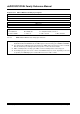
Register 43-15: SPHASEx: PWM Secondary Phase Shift Register
R/W-0 R/W-0 R/W-0 R/W-0 R/W-0 R/W-0 R/W-0 R/W-0
SPHASEx<15:8>
bit 15 bit 8
R/W-0 R/W-0 R/W-0 R/W-0 R/W-0 R/W-0 R/W-0 R/W-0
SPHASEx<7:0>
bit 7 bit 0
Legend:
R = Readable bit W = Writable bit U = Unimplemented bit, read as ‘0’
-n = Value at POR ‘1’ = Bit is set ‘0’ = Bit is cleared x = Bit is unknown
bit 15-0 SPHASEx<15:0>: Secondary Phase Offset bits for the PWMxL Output Pin (used in Independent
PWM mode only)
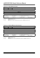
Note 1: If PWMCONx<9> = 0, the following applies based on the mode of operation:
• Complementary, Redundant and Push-Pull PWM Output mode (IOCONx<11:10> = 00, 01 or 10)
SPHASEx<15:0> = Not used.
• True Independent PWM Output mode (IOCONx<11:10> = 11) SPHASEx<15:0> = Phase shift value
for PWMxL only.
• When the PHASEx/SPHASEx register provides the phase shift with respect to the master time
base, the valid range of values is 0x0000 – Period.
2: If PWMCONx<9> = 1, the following applies based on the mode of operation:
• Complementary, Redundant and Push-Pull PWM Output mode (IOCONx<11:10> = 00, 01 or 10)
SPHASEx<15:0> = Not used.
• True Independent PWM Output mode (IOCONx<11:10> = 11) SPHASEx<15:0> = Independent time
base period value for PWMxL only.
• When PHASEx/SPHASEx register provides the local period, the valid range of values
are0x0010–0xFFF8.