
Specifications


© 2008-2012 Microchip Technology Inc. DS70323E-page 43-17
Section 43. High-Speed PWM
High-Speed PWM
43
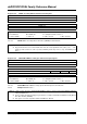
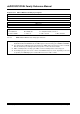
Register 43-13: SDCx: PWM Secondary Duty Cycle Register
R/W-0 R/W-0 R/W-0 R/W-0 R/W-0 R/W-0 R/W-0 R/W-0
SDCx<15:8>
bit 15 bit 8
R/W-0 R/W-0 R/W-0 R/W-0 R/W-0 R/W-0 R/W-0 R/W-0
SDCx<7:0>
bit 7 bit 0
Legend:
R = Readable bit W = Writable bit U = Unimplemented bit, read as ‘0’
-n = Value at POR ‘1’ = Bit is set ‘0’ = Bit is cleared x = Bit is unknown
bit 15-0 SDCx<15:0>: Secondary Duty Cycle bits for the PWMxL Output Pin
Note 1: The SDCx register is used in Independent Output mode only. When used in Independent Output mode,
the SDCx register controls the PWMxL duty cycle. This register is ignored in other PWM modes.
2: The smallest pulse width that can be generated on the PWM output corresponds to a value of 0x0008,
while the maximum pulse width generated corresponds to a value of Period + 0x0008.
3: SDCx < 0x0008 produces 0% duty cycle. SDCx > Period + 0x0008 produces 100% duty cycle.
4: As the Duty Cycle gets closer to 0% or 100% of the PWM Period (0 ns to 40 ns, depending on the mode
of operation), PWM Duty Cycle resolution will increase from 1 LSb to 3 LSbs.