
Specifications


dsPIC33F/PIC24H Family Reference Manual
DS70323E-page 43-14 © 2008-2012 Microchip Technology Inc.
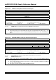
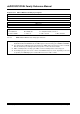
Register 43-11: PWMCONx: PWM Control Register
HS/HC-0 HS/HC-0 HS/HC-0 R/W-0 R/W-0 R/W-0 R/W-0 R/W-0
FLTSTAT
(1)
CLSTAT
(1)
TRGSTAT FLTIEN CLIEN TRGIEN ITB
(3)
MDCS
(3)
bit 15 bit 8
R/W-0 R/W-0 R/W-0 U-0 R/W-0 R/W-0 R/W-0 R/W-0
DTC<1:0>
(3)
DTCP
(3,6)
—MTBSCAM
(2,3,5)
XPRES
(4)
IUE
bit 7 bit 0
Legend: HC = Cleared in Hardware HS = Set in Hardware
R = Readable bit W = Writable bit U = Unimplemented bit, read as ‘0’
-n = Value at POR ‘1’ = Bit is set ‘0’ = Bit is cleared x = Bit is unknown
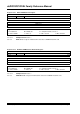
bit 15 FLTSTAT: Fault Interrupt Status bit
(1)
1 = Fault interrupt is pending
0 = No Fault interrupt is pending
This bit is cleared by setting FLTIEN = 0.
bit 14 CLSTAT: Current-Limit Interrupt Status bit
(1)
1 = Current-limit interrupt is pending
0 = No current-limit interrupt is pending
This bit is cleared by setting CLIEN = 0.
bit 13 TRGSTAT: Trigger Interrupt Status bit
1 = Trigger interrupt is pending
0 = No trigger interrupt is pending
This bit is cleared by setting TRGIEN = 0.
bit 12 FLTIEN: Fault Interrupt Enable bit
1 = Fault interrupt is enabled
0 = Fault interrupt is disabled and FLTSTAT bit is cleared
bit 11 CLIEN: Current-Limit Interrupt Enable bit
1 = Current-limit interrupt enabled
0 = Current-limit interrupt disabled and CLSTAT bit is cleared
bit 10 TRGIEN: Trigger Interrupt Enable bit
1 = A trigger event generates an IRQ
0 = Trigger event interrupts are disabled and TRGSTAT bit is cleared
bit 9 ITB: Independent Time Base Mode bit
(3)
1 = PHASEx/SPHASEx registers provide time base period for this PWM generator
0 = PTPER/STPER register provides timing for this PWM generator
bit 8 MDCS: Master Duty Cycle Register Select bit
(3)
1 = MDC register provides duty cycle information for this PWM generator
0 = PDCx and SDCx registers provide duty cycle information for this PWM generator
Note 1: Software must clear the interrupt status, and the corresponding IFS bit in the Interrupt Controller.
2: The Independent Time Base mode (ITB = 1) must be enabled to use Center-Aligned mode. If ITB = 0, the
CAM bit is ignored.
3: These bits should not be changed after the PWM is enabled (PTEN = 1).
4: Configure FCLCON
X<8> = 0 and PWMCONX<9> = 1, to operate in External Period Reset mode.
5: Center-aligned mode ignores the Least Significant 3 bits of the duty cycle, phase and dead time registers.
The highest CAM resolution available is 8.32 ns with the clock prescaler set to the fastest clock.
6: DTC<1:0> = 11 for DTCP to be effective; otherwise, DTCP is ignored.