
Specifications


© 2008-2012 Microchip Technology Inc. DS70323E-page 43-13
Section 43. High-Speed PWM
High-Speed PWM
43
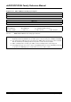
Register 43-9: CHOP: PWM Chop Clock Generator Register
R/W-0 U-0 U-0 U-0 U-0 U-0 R/W-0 R/W-0
CHPCLKEN
— — — — — CHOP<6:5>
bit 15 bit 8
R/W-0 R/W-0 R/W-0 R/W-0 R/W-0 U-0 U-0 U-0
CHOP<4:0>
— — —
bit 7 bit 0
Legend:
R = Readable bit W = Writable bit U = Unimplemented bit, read as ‘0’
-n = Value at POR ‘1’ = Bit is set ‘0’ = Bit is cleared x = Bit is unknown
bit 15 CHPCLKEN: Enable Chop Clock Generator bit
1 = Chop clock generator is enabled
0 = Chop clock generator is disabled
bit 14-10 Unimplemented: Read as ‘0’
bit 9-3 CHOP<6:0>: Chop Clock Divider bits
Value in 8.32 ns increments. The frequency of the chop clock signal is calculated as follows:
Chop Frequency = 1/(16.64 * (CHOP<6:0> + 1) * Primary Master PWM Input Clock/PCLKDIV<2:0>
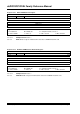
Register 43-10: MDC: PWM Master Duty Cycle Register
R/W-0 R/W-0 R/W-0 R/W-0 R/W-0 R/W-0 R/W-0 R/W-0
MDC<15:8>
bit 15 bit 8
R/W-0 R/W-0 R/W-0 R/W-0 R/W-0 R/W-0 R/W-0 R/W-0
MDC<7:0>
bit 7 bit 0
Legend:
R = Readable bit W = Writable bit U = Unimplemented bit, read as ‘0’
-n = Value at POR ‘1’ = Bit is set ‘0’ = Bit is cleared x = Bit is unknown
bit 15-0 MDC<15:0>: Master PWM Duty Cycle Value bits
Note 1: The smallest pulse width that can be generated on the PWM output corresponds to a value of 0x0008,
while the maximum pulse width generated corresponds to a value of Period + 0x0008.
2: MDC < 0x0008 will produce 0% duty cycle. MDC > Period + 0x0008 will produce 100% duty cycle.
3: As the Duty Cycle gets closer to 0% or 100% of the PWM Period (0 ns to 40 ns, depending on the mode
of operation), PWM Duty Cycle resolution will increase from 1 LSb to 3 LSbs.