
Specifications


© 2008-2012 Microchip Technology Inc. DS70323E-page 43-103
Section 43. High-Speed PWM
High-Speed PWM
43
43.17 BURST MODE IMPLEMENTATION
In applications where the load current drawn from the converter is much smaller than its nominal
current/converter operating at no load, the power drawn from the source can be reduced by
forcing the converter into Discontinuous mode. This is achieved by deasserting the PWM outputs
for a specific amount of time using the manual override feature.
Typically, the converter PWM output can be turned off over a period of time based on the output
voltage regulation, which can reduce the no load power requirements significantly.
43.18 PWM INTERCONNECTS WITH OTHER PERIPHERALS
(ADC, ANALOG COMPARATOR AND INTERRUPT CONTROLLER)
Most power conversion applications require close synchronization of the PWM module with other
peripherals, such as the High-Speed 10-bit ADC and the High-Speed Analog Comparator. Due
to the critical timing requirements for power conversion applications, this interconnection must
be accomplished with little or no CPU overhead. The interconnection should also ensure a fast
response time, often in the order of nanoseconds.
The High-Speed PWM module contains a number of enhancements for direct interconnects with
the High-Speed 10-bit ADC and the High-Speed Analog Comparator modules. This section
describes each of these enhancements and also identifies examples where these enhancements
are beneficial for power conversion applications.
43.18.1 PWM – ADC Interconnect
43.18.1.1 PRECISE TRIGGERING OF ADC
In digital power supplies, the ADC is used for measurement of feedback signals. These feedback
signals can have complex waveforms or high noise content; therefore, precise triggering of the
ADC is important.
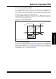
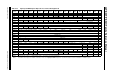
Incorrect triggering of the ADC could have a major impact on the operation of the power
converter. As an example, Figure 43-55 illustrates a DC-DC boost converter with the current
sensor located in series with the source pin of the power MOSFET. This configuration eliminates
the need for a differential amplifier with a high common mode voltage capability, and therefore,
provides a low cost sensing solution. The trade-off is that the ADC only sees the MOSFET
current.
If the digital control system is configured to measure the peak current, a small delay in triggering
the ADC will yield a result of 0x0000. This delay may be caused by software overheads or if the
ADC is busy at the sampling instant.
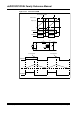
Figure 43-55: Need for Precise ADC Triggering
X
PWM
I
L
IR
X
X
Late sample yields zero data
Desired sample point
Critical Edge
+VIN
IL
L
PWM
V
ISENSE
VOUT
COUT
+
I
R
R
Note: Measuring peak inductor current is very important.
Example Boost Converter