
Information


Table Of Contents
- TABLE 1: Silicon DEVREV Values (Continued)
- TABLE 2: Silicon Issue Summary (Continued)
- Silicon Errata Issues
- 1. Module: I/O Multiplexer
- 2. Module: CPU
- 3. Module: CPU
- 4. Module: PPS
- 5. Module: SPI
- 6. Module: SPI
- 7. Module: PWM
- 8. Module: PWM
- 9. Module: Power System
- 10. Module: Reserved
- 11. Module: ECAN™
- 12. Module: ECAN
- 13. Module: USB
- 14. Module: USB
- 15. Module: DMA
- 16. Module: UART
- 17. Module: UART
- 18. Module: UART
- 19. Module: I2C™
- 20. Module: ADC
- 21. Module: PMP
- 22. Module: Flash Memory
- 23. Module: Flash Memory
- 24. Module: Power System
- 25. Module: PWM
- 26. Module: QEI
- 27. Module: QEI
- 28. Module: CPU
- 29. Module: PWM
- 30. Module: ECAN
- 31. Module: Auxiliary Flash
- 32. Module: Auxiliary Flash
- 33. Module: Output Compare
- 34. Module: ADC
- Data Sheet Clarifications
- Appendix A: Revision History
dsPIC33EPXXX(GP/MC/MU)806/810/814 and PIC24EPXXX(GP/GU)810/814
DS80526C-page 10 © 2011-2012 Microchip Technology Inc.
17. Module: UART
When a Read-Modify-Write operation is performed
to set or clear any bit(s) in the UxSTA register while
hardware is clearing the UTXBRK bit (UxSTA<11>),
the UTXBRK bit may remain set. BSET and BCLR
are examples of Read-Modify-Write instructions.
Work around
Wait for the UTXBRK bit to get cleared by
hardware, before performing a Read-Modify-Write
operation on the UxSTA register.
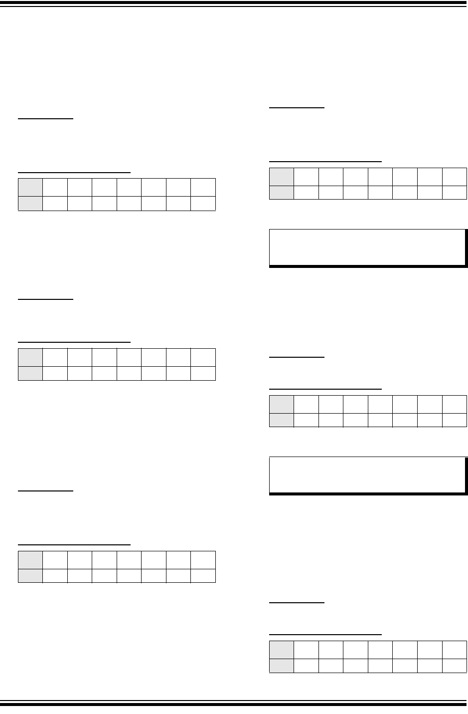
Affected Silicon Revisions
18. Module: UART
The transmitter write pointer does not get cleared
when the UART module is disabled
(UARTEN = 0), and it requires the TXEN bit to be
set in order to clear the write pointer.
Work around
Do not load data into the TX FIFO (register) before
setting the TXEN bit.
Affected Silicon Revisions
19. Module: I
2
C™
When a Read-Modify-Write operation is performed
to set or clear any bit(s) in the I2CxCON register
while hardware is clearing the ACKEN bit
(I2CxCON<4>), the ACKEN bit may remain set.
BSET and BCLR are examples of Read-Modify-Write
instructions.
Work around
Wait for the ACKEN bit to get cleared by hardware
before performing a Read-Modify-Write operation
on the I2CxCON register.
Affected Silicon Revisions
20. Module: ADC
The ADC Conversion Status bit, DONE
(ADxCON1<0>), does not indicate completion of
conversion when External Interrupt is selected as
the ADC trigger source (ADxCON1<SSRC> = 1).
Work around
Use ADC interrupt or poll ADxIF (in the IFSx
registers) bit to determine the completion of
conversion.
Affected Silicon Revisions
21. Module: PMP
When PTEN14 = 1 (PMAEN<14>), the PMA<14> or
PMCS1 functionality is present on the PMCS1/RK11
(pin 94) and RJ14 (pin 21).
When PTEN15 = 1 (PMAEN<15>), the PMA<15> or
PMCS2 functionality is present on the PMCS2/
RK12 (pin 93) and RJ15 (pin 22).
Work around
None.
Affected Silicon Revisions
22. Module: Flash Memory
If code or write protection is enabled on either the
General Segment or Auxiliary Segment, neither
segment can be read by the programmer. Code or
write protection is enabled for the General Segment
when the GSS (FGS<1>) or GWRP (FGS<0>) bits
are ‘0’. Code or write protection is enabled for the
Auxiliary Segment when the APL (FAS<1>) or
AWRP (FAS<0>) bits are ‘0’.
Work around
None.
Affected Silicon Revisions
B1
X
B1
X
B1
X
B1
X
Note: This silicon issue applies only to
dsPIC33EPXXXMU814 and
PIC24EPXXXMC814 devices.
B1
X
Note: This silicon issue applies only to In-
Circuit Serial Programming™
(ICSP™) mode.
B1
X