
Datasheet


dsPIC33EPXXX(GP/MC/MU)806/810/814 and PIC24EPXXX(GP/GU)810/814
DS70616G-page 516 2009-2012 Microchip Technology Inc.
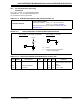
FIGURE 32-4: POWER-ON RESET TIMING CHARACTERISTICS
VDD
VPOR
Note 1: The power-up period will be extended if the power-up sequence completes before the device exits from BOR
(V
DD < VBOR).
2: The power-up period includes internal voltage regulator stabilization delay.
SY00
Power-up Sequence
V
DD
VPOR
Power-up Timer Enabled – Clock Sources = (FRC, FRCDIVN, FRCDIV16, FRCPLL, EC, ECPLL and LPRC)
Power-up Timer Disabled – Clock Sources = (HS, HSPLL, XT, XTPLL and SOSC)
(T
PU
)
SY10
SY11
Power-up Sequence
(Note 1,2)
CPU Starts Fetching Code
CPU Starts Fetching Code
(T
PWRT
)
VDD
VPOR
SY00
Power-up Sequence
Power-up Timer Disabled – Clock Sources = (FRC, FRCDIVN, FRCDIV16, FRCPLL, EC, ECPLL and LPRC)
(T
PU
)
CPU Starts Fetching Code
(Note 1,2)
(Note 1,2)
(T
OST
)
SY00
(T
PU
)
VDD
VPOR
Power-up Timer Enabled – Clock Sources = (HS, HSPLL, XT, XTPLL and SOSC)
Greater of
Power-up Sequence
(Note 1,2)
CPU Starts Fetching Code
SY00
(T
PU
)
SY11 (T
PWRT
)
SY10 (T
OST
)
or