
Datasheet


Table Of Contents
- High-Performance Modified RISC CPU:
- DSP Features:
- Peripheral Features:
- Analog Features:
- Special Microcontroller Features:
- CMOS Technology:
- dsPIC30F6011A/6012A/6013A/6014A Controller Families
- Pin Diagrams
- Pin Diagrams (Continued)
- Pin Diagrams (Continued)
- Pin Diagrams (Continued)
- Table of Contents
- Most Current Data Sheet
- Errata
- Customer Notification System
- 1.0 Device Overview
- 2.0 CPU Architecture Overview
- 3.0 Memory Organization
- 3.1 Program Address Space
- FIGURE 3-1: program space memory map FOR dsPIC30F6011A/ 6013A
- FIGURE 3-2: program space memory map FOR dsPIC30F6012A/ 6014A
- TABLE 3-1: Program Space Address Construction
- FIGURE 3-3: DATA ACCESS FROM PROGRAM SPACE ADDRESS GENERATION
- 3.1.1 Data Access From Program Memory using Table Instructions
- 3.1.2 Data Access From Program Memory using Program Space Visibility
- 3.2 Data Address Space
- 3.1 Program Address Space
- 4.0 Address Generator Units
- 5.0 Interrupts
- 6.0 Flash Program Memory
- 6.1 In-Circuit Serial Programming (ICSP)
- 6.2 Run-Time Self-Programming (RTSP)
- 6.3 Table Instruction Operation Summary
- 6.4 RTSP Operation
- 6.5 Control Registers
- 6.6 Programming Operations
- 7.0 Data EEPROM Memory
- 8.0 I/O Ports
- 8.1 Parallel I/O (PIO) Ports
- 8.2 Configuring Analog Port Pins
- FIGURE 8-2: Block Diagram of a ShAred PORT Structure
- TABLE 8-1: PORTA Register MAp for dsPIC30F6013A/6014A(1)
- TABLE 8-2: PORTB Register MAp for dsPIC30F6011A/6012A/6013A/6014A(1)
- TABLE 8-3: PORTC Register MAp for dsPIC30F6011A/6012A(1)
- TABLE 8-4: PORTC Register MAp for dsPIC30F6013A/6014A(1)
- TABLE 8-5: PORTD Register MAp for dsPIC30F6011A/6012A(1)
- TABLE 8-6: PORTD Register MAp for dsPIC30F6013A/6014A(1)
- TABLE 8-7: PORTF Register MAp for dsPIC30F6011A/6012A(1)
- TABLE 8-8: PORTF Register MAp for dsPIC30F6013A/6014A(1)
- TABLE 8-9: PORTG Register MAp for dsPIC30F6011A/6012A/6013A/6014A(1)
- 8.3 Input Change Notification Module
- TABLE 8-10: Input change notification register map for dsPIC30F6011A/6012A (Bits 15-8)(1)
- TABLE 8-11: Input Change notification register map FOR dsPIC30F6011A/6012A (Bits 7-0)(1)
- TABLE 8-12: Input change notification register map for dsPIC30F6013A/6014A (Bits 15-8)(1)
- TABLE 8-13: Input Change notification register map FOR dsPIC30F6013A/6014A (Bits 7-0)(1)
- 9.0 Timer1 Module
- 10.0 Timer2/3 Module
- 11.0 Timer4/5 Module
- 12.0 Input Capture Module
- 13.0 Output Compare Module
- FIGURE 13-1: Output Compare Mode Block DiagrAm
- 13.1 Timer2 and Timer3 Selection Mode
- 13.2 Simple Output Compare Match Mode
- 13.3 Dual Output Compare Match Mode
- 13.4 Simple PWM Mode
- 13.5 Output Compare Operation During CPU Sleep Mode
- 13.6 Output Compare Operation During CPU Idle Mode
- 13.7 Output Compare Interrupts
- 14.0 SPI™ Module
- 15.0 I2C™ Module
- 15.1 Operating Function Description
- 15.2 I2C Module Addresses
- 15.3 I2C 7-bit Slave Mode Operation
- 15.4 I2C 10-bit Slave Mode Operation
- 15.5 Automatic Clock Stretch
- 15.6 Software Controlled Clock Stretching (STREN = 1)
- 15.7 Interrupts
- 15.8 Slope Control
- 15.9 IPMI Support
- 15.10 General Call Address Support
- 15.11 I2C Master Support
- 15.12 I2C Master Operation
- 15.13 I2C Module Operation During CPU Sleep and Idle Modes
- 16.0 Universal Asynchronous Receiver Transmitter (UART) Module
- 17.0 CAN Module
- 18.0 Data Converter Interface (DCI) Module
- 18.1 Module Introduction
- 18.2 Module I/O Pins
- 18.3 DCI Module Operation
- 18.3.1 MODULE ENABLE
- 18.3.2 Word Size Selection Bits
- 18.3.3 Frame SYNC GEnerator
- 18.3.4 Frame Sync Mode Control Bits
- 18.3.5 Master frame sync Operation
- 18.3.6 Slave Frame Sync Operation
- 18.3.7 Bit Clock Generator
- 18.3.8 Sample Clock Edge control Bit
- 18.3.9 Data Justification Control bit
- 18.3.10 Transmit Slot Enable Bits
- 18.3.11 Receive Slot Enable Bits
- 18.3.12 Slot Enable Bits Operation with FRame SYNC
- 18.3.13 Synchronous data transfers
- 18.3.14 Buffer Length Control
- 18.3.15 Buffer Alignment With Data Frames
- 18.3.16 Transmit STATUS BITS
- 18.3.17 RECEIVE STATUS bits
- 18.3.18 SLOT Status Bits
- 18.3.19 CSDO Mode Bit
- 18.3.20 Digital Loopback mode
- 18.3.21 Underflow Mode Control Bit
- 18.4 DCI Module Interrupts
- 18.5 DCI Module Operation During CPU Sleep and Idle Modes
- 18.6 AC-Link Mode Operation
- 18.7 I2S Mode Operation
- 19.0 12-bit Analog-to-Digital Converter (ADC) Module
- FIGURE 19-1: 12-bit ADC Functional Block Diagram
- 19.1 ADC Result Buffer
- 19.2 Conversion Operation
- 19.3 Selecting the Conversion Sequence
- 19.4 Programming the Start of Conversion Trigger
- 19.5 Aborting a Conversion
- 19.6 Selecting the ADC Conversion Clock
- 19.7 ADC Speeds
- 19.8 ADC Acquisition Requirements
- 19.9 Module Power-down Modes
- 19.10 ADC Operation During CPU Sleep and Idle Modes
- 19.11 Effects of a Reset
- 19.12 Output Formats
- 19.13 Configuring Analog Port Pins
- 19.14 Connection Considerations
- 20.0 System Integration
- 20.1 Oscillator System Overview
- 20.2 Oscillator Configurations
- 20.3 Oscillator Control Registers
- 20.4 Reset
- 20.5 Watchdog Timer (WDT)
- 20.6 Low-Voltage Detect
- 20.7 Power-Saving Modes
- 20.8 Device Configuration Registers
- 20.9 Peripheral Module Disable (PMD) Registers
- 20.10 In-Circuit Debugger
- 21.0 Instruction Set Summary
- 22.0 Development Support
- 22.1 MPLAB Integrated Development Environment Software
- 22.2 MPLAB C Compilers for Various Device Families
- 22.3 HI-TECH C for Various Device Families
- 22.4 MPASM Assembler
- 22.5 MPLINK Object Linker/ MPLIB Object Librarian
- 22.6 MPLAB Assembler, Linker and Librarian for Various Device Families
- 22.7 MPLAB SIM Software Simulator
- 22.8 MPLAB REAL ICE In-Circuit Emulator System
- 22.9 MPLAB ICD 3 In-Circuit Debugger System
- 22.10 PICkit 3 In-Circuit Debugger/ Programmer and PICkit 3 Debug Express
- 22.11 PICkit 2 Development Programmer/Debugger and PICkit 2 Debug Express
- 22.12 MPLAB PM3 Device Programmer
- 22.13 Demonstration/Development Boards, Evaluation Kits, and Starter Kits
- 23.0 Electrical Characteristics
- Absolute Maximum Ratings(†)
- 23.1 DC Characteristics
- TABLE 23-1: Operating MIPS vs. Voltage
- TABLE 23-2: Thermal Operating Conditions
- TABLE 23-3: Thermal Packaging Characteristics
- TABLE 23-4: DC Temperature and Voltage specifications
- TABLE 23-5: DC Characteristics: Operating Current (Idd)
- TABLE 23-6: DC Characteristics: Idle Current (iidle)
- TABLE 23-7: DC Characteristics: Power-Down Current (Ipd)
- TABLE 23-8: DC Characteristics: I/O Pin Input Specifications
- TABLE 23-9: DC Characteristics: I/O Pin Output Specifications
- FIGURE 23-1: Low-Voltage Detect Characteristics
- TABLE 23-10: Electrical Characteristics: LVDL
- FIGURE 23-2: Brown-out Reset Characteristics
- TABLE 23-11: Electrical Characteristics: BOR
- TABLE 23-12: DC Characteristics: Program and EEPROM
- 23.2 AC Characteristics and Timing Parameters
- TABLE 23-13: Temperature and Voltage Specifications – AC
- FIGURE 23-3: Load Conditions for Device Timing Specifications
- FIGURE 23-4: External Clock Timing
- TABLE 23-14: External Clock Timing Requirements
- TABLE 23-15: PLL Clock Timing Specifications (Vdd = 2.5 to 5.5 V)
- TABLE 23-16: PLL Jitter
- TABLE 23-17: Internal Clock Timing examples
- TABLE 23-18: AC Characteristics: Internal FRC Accuracy
- TABLE 23-19: AC Characteristics: Internal LPRC accuracy
- FIGURE 23-5: CLKOUT and I/O Timing Characteristics
- TABLE 23-20: CLKOUT and I/O Timing Requirements
- FIGURE 23-6: Reset, Watchdog Timer, Oscillator Start-up Timer and Power-up Timer Timing Characteristics
- TABLE 23-21: Reset, Watchdog Timer, Oscillator Start-up Timer, Power-up Timer and Brown-out Reset Timing Requirements
- FIGURE 23-7: band gap Start-up Time Characteristics
- TABLE 23-22: band gap Start-up Time Requirements
- FIGURE 23-8: Type A, B and C Timer External Clock Timing Characteristics
- TABLE 23-23: TYPE A TIMER (Timer1) External Clock Timing Requirements(1)
- TABLE 23-24: TYPE B TIMER (Timer2 and Timer4) External Clock Timing Requirements(1)
- TABLE 23-25: TYPE C TIMER (Timer3 and Timer5) External Clock Timing Requirements(1)
- FIGURE 23-9: INPUT CAPTURE (CAPx) TIMING Characteristics
- TABLE 23-26: Input Capture timing requirements
- FIGURE 23-10: Output Compare Module (OCx) Timing Characteristics
- TABLE 23-27: Output Compare Module timing requirements
- FIGURE 23-11: OC/PWM Module Timing Characteristics
- TABLE 23-28: Simple OC/PWM MODE Timing Requirements
- FIGURE 23-12: DCI Module (Multichannel, I2S modes) Timing Characteristics
- TABLE 23-29: DCI Module (Multichannel, I2S modes) Timing Requirements
- FIGURE 23-13: DCI Module (AC-link mode) Timing Characteristics
- TABLE 23-30: DCI Module (AC-Link Mode) Timing Requirements
- FIGURE 23-14: SPI Module Master Mode (CKE = 0) Timing Characteristics
- TABLE 23-31: SPI Master mode (cke = 0) Timing requirements
- FIGURE 23-15: SPI Module Master Mode (CKE =1) Timing Characteristics
- TABLE 23-32: SPI Module Master mode (cke = 1) Timing requirements
- FIGURE 23-16: SPI Module Slave Mode (CKE = 0) Timing Characteristics
- TABLE 23-33: SPI Module Slave mode (cke = 0) Timing requirements
- FIGURE 23-17: SPI Module Slave Mode (CKE = 1) Timing Characteristics
- TABLE 23-34: SPI Module Slave mode (cke = 1) Timing requirements
- FIGURE 23-18: I2C™ Bus Start/Stop Bits Timing Characteristics (Master mode)
- FIGURE 23-19: I2C™ Bus Data Timing Characteristics (Master mode)
- TABLE 23-35: I2C™ Bus Data Timing Requirements (Master Mode)
- FIGURE 23-20: I2C™ Bus Start/Stop Bits Timing Characteristics (slave mode)
- FIGURE 23-21: I2C™ Bus Data Timing Characteristics (slave mode)
- TABLE 23-36: I2C™ Bus Data Timing Requirements (Slave Mode)
- FIGURE 23-22: CAN Module I/O Timing Characteristics
- TABLE 23-37: CAN Module I/O Timing Requirements
- TABLE 23-38: 12-bit ADC Module Specifications
- FIGURE 23-23: 12-Bit ADC Timing Characteristics (asam = 0, ssrc = 000)
- TABLE 23-39: 12-BIT ADC TiminG rEQUIREMENTS
- 24.0 Packaging Information
- Appendix A: Revision History
- Index
- The Microchip Web Site
- Customer Change Notification Service
- Customer Support
- Reader Response
- Product Identification System
© 2011 Microchip Technology Inc. DS70143E-page 167
dsPIC30F6011A/6012A/6013A/6014A
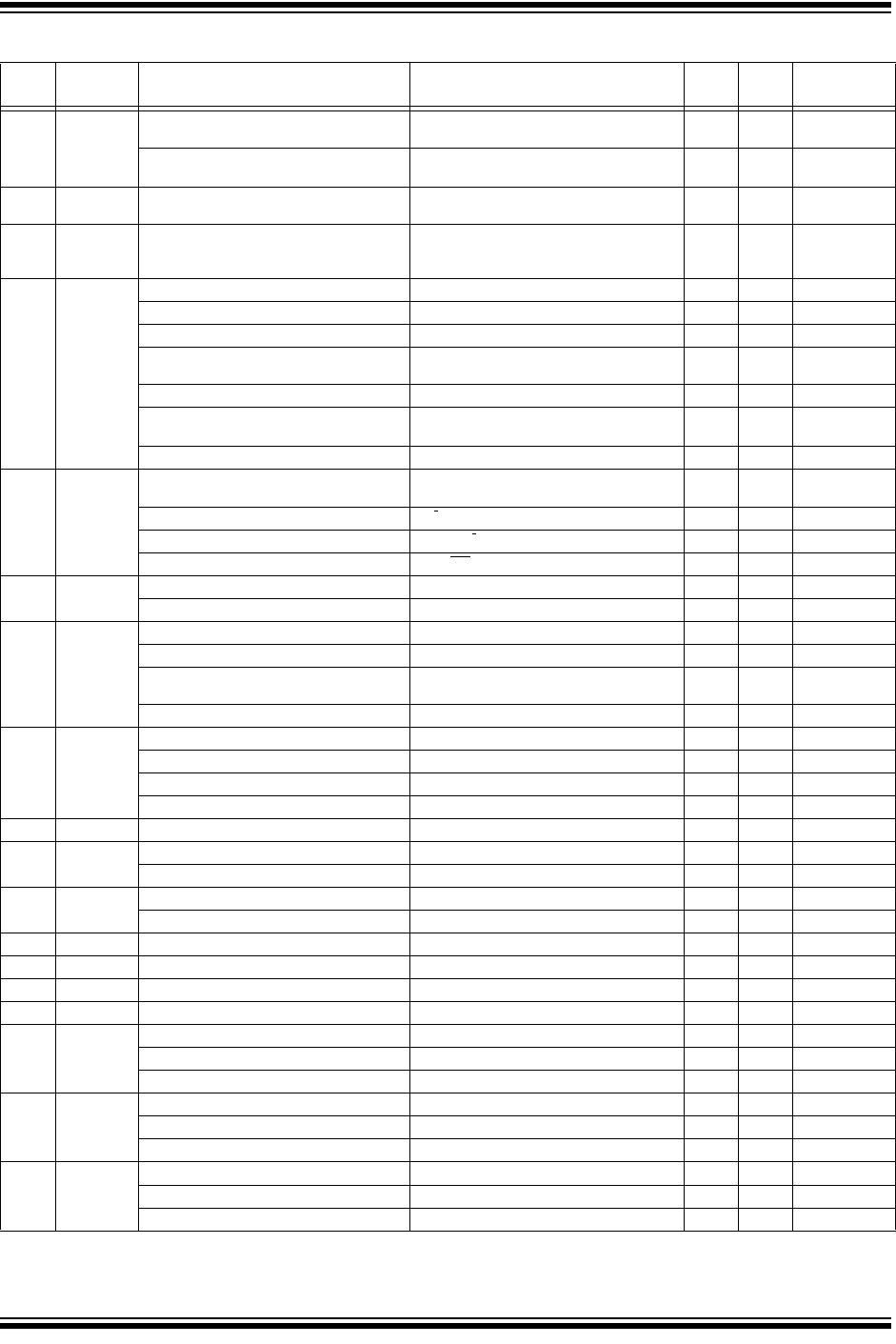
48 MPY MPY
Wm*Wn,Acc,Wx,Wxd,Wy,Wyd
Multiply Wm by Wn to Accumulator 1 1 OA,OB,OAB,
SA,SB,SAB
MPY
Wm*Wm,Acc,Wx,Wxd,Wy,Wyd
Square Wm to Accumulator 1 1 OA,OB,OAB,
SA,SB,SAB
49 MPY.N MPY.N
Wm*Wn,Acc,Wx,Wxd,Wy,Wyd
-(Multiply Wm by Wn) to Accumulator 1 1 None
50 MSC MSC Wm*Wm,Acc,Wx,Wxd,Wy,Wyd
,
AWB
Multiply and Subtract from Accumulator 1 1 OA,OB,OAB,
SA,SB,SAB
51 MUL MUL.SS Wb,Ws,Wnd {Wnd + 1, Wnd} = signed(Wb) * signed(Ws) 1 1 None
MUL.SU Wb,Ws,Wnd {Wnd + 1, Wnd} = signed(Wb) * unsigned(Ws) 1 1 None
MUL.US Wb,Ws,Wnd {Wnd + 1, Wnd} = unsigned(Wb) * signed(Ws) 1 1 None
MUL.UU Wb,Ws,Wnd {Wnd + 1, Wnd} = unsigned(Wb) *
unsigned(Ws)
11 None
MUL.SU Wb,#lit5,Wnd {Wnd + 1, Wnd} = signed(Wb) * unsigned(lit5) 1 1 None
MUL.UU Wb,#lit5,Wnd {Wnd + 1, Wnd} = unsigned(Wb) *
unsigned(lit5)
11 None
MUL f W3:W2 = f * WREG 1 1 None
52 NEG NEG Acc Negate Accumulator 1 1 OA,OB,OAB,
SA,SB,SAB
NEG f f = f
+ 1 1 1 C,DC,N,OV,Z
NEG f,WREG WREG = f
+ 1 1 1 C,DC,N,OV,Z
NEG Ws,Wd Wd = Ws
+ 1 1 1 C,DC,N,OV,Z
53 NOP NOP No Operation 1 1 None
NOPR No Operation 1 1 None
54 POP POP f Pop f from Top-of-Stack (TOS) 1 1 None
POP Wdo Pop from Top-of-Stack (TOS) to Wdo 1 1 None
POP.D Wnd Pop from Top-of-Stack (TOS) to
W(nd):W(nd+1)
12 None
POP.S Pop Shadow Registers 1 1 All
55 PUSH PUSH f Push f to Top-of-Stack (TOS) 1 1 None
PUSH Wso Push Wso to Top-of-Stack (TOS) 1 1 None
PUSH.D Wns Push W(ns):W(ns+1) to Top-of-Stack (TOS) 1 2 None
PUSH.S Push Shadow Registers 1 1 None
56 PWRSAV PWRSAV #lit1 Go into Sleep or Idle mode 1 1 WDTO,Sleep
57 RCALL RCALL Expr Relative Call 1 2 None
RCALL Wn Computed Call 1 2 None
58 REPEAT REPEAT #lit14 Repeat Next Instruction lit14 + 1 times 1 1 None
REPEAT Wn Repeat Next Instruction (Wn) + 1 times 1 1 None
59 RESET RESET Software device Reset 1 1 None
60 RETFIE RETFIE Return from interrupt 1 3 (2) None
61 RETLW RETLW #lit10,Wn Return with literal in Wn 1 3 (2) None
62 RETURN RETURN Return from Subroutine 1 3 (2) None
63 RLC RLC f f = Rotate Left through Carry f 1 1 C,N,Z
RLC f,WREG WREG = Rotate Left through Carry f 1 1 C,N,Z
RLC Ws,Wd Wd = Rotate Left through Carry Ws 1 1 C,N,Z
64 RLNC RLNC f f = Rotate Left (No Carry) f 1 1 N,Z
RLNC f,WREG WREG = Rotate Left (No Carry) f 1 1 N,Z
RLNC Ws,Wd Wd = Rotate Left (No Carry) Ws 1 1 N,Z
65 RRC RRC f f = Rotate Right through Carry f 1 1 C,N,Z
RRC f,WREG WREG = Rotate Right through Carry f 1 1 C,N,Z
RRC Ws,Wd Wd = Rotate Right through Carry Ws 1 1 C,N,Z
TABLE 21-2: INSTRUCTION SET OVERVIEW (CONTINUED)
Base
Instr #
Assembly
Mnemonic
Assembly Syntax Description # of
Words
# of
Cycles
Status Flags
Affected