
Datasheet


Table Of Contents
- High-Performance Modified RISC CPU:
- DSP Features:
- Peripheral Features:
- Analog Features:
- Special Microcontroller Features:
- CMOS Technology:
- dsPIC30F6011A/6012A/6013A/6014A Controller Families
- Pin Diagrams
- Pin Diagrams (Continued)
- Pin Diagrams (Continued)
- Pin Diagrams (Continued)
- Table of Contents
- Most Current Data Sheet
- Errata
- Customer Notification System
- 1.0 Device Overview
- 2.0 CPU Architecture Overview
- 3.0 Memory Organization
- 3.1 Program Address Space
- FIGURE 3-1: program space memory map FOR dsPIC30F6011A/ 6013A
- FIGURE 3-2: program space memory map FOR dsPIC30F6012A/ 6014A
- TABLE 3-1: Program Space Address Construction
- FIGURE 3-3: DATA ACCESS FROM PROGRAM SPACE ADDRESS GENERATION
- 3.1.1 Data Access From Program Memory using Table Instructions
- 3.1.2 Data Access From Program Memory using Program Space Visibility
- 3.2 Data Address Space
- 3.1 Program Address Space
- 4.0 Address Generator Units
- 5.0 Interrupts
- 6.0 Flash Program Memory
- 6.1 In-Circuit Serial Programming (ICSP)
- 6.2 Run-Time Self-Programming (RTSP)
- 6.3 Table Instruction Operation Summary
- 6.4 RTSP Operation
- 6.5 Control Registers
- 6.6 Programming Operations
- 7.0 Data EEPROM Memory
- 8.0 I/O Ports
- 8.1 Parallel I/O (PIO) Ports
- 8.2 Configuring Analog Port Pins
- FIGURE 8-2: Block Diagram of a ShAred PORT Structure
- TABLE 8-1: PORTA Register MAp for dsPIC30F6013A/6014A(1)
- TABLE 8-2: PORTB Register MAp for dsPIC30F6011A/6012A/6013A/6014A(1)
- TABLE 8-3: PORTC Register MAp for dsPIC30F6011A/6012A(1)
- TABLE 8-4: PORTC Register MAp for dsPIC30F6013A/6014A(1)
- TABLE 8-5: PORTD Register MAp for dsPIC30F6011A/6012A(1)
- TABLE 8-6: PORTD Register MAp for dsPIC30F6013A/6014A(1)
- TABLE 8-7: PORTF Register MAp for dsPIC30F6011A/6012A(1)
- TABLE 8-8: PORTF Register MAp for dsPIC30F6013A/6014A(1)
- TABLE 8-9: PORTG Register MAp for dsPIC30F6011A/6012A/6013A/6014A(1)
- 8.3 Input Change Notification Module
- TABLE 8-10: Input change notification register map for dsPIC30F6011A/6012A (Bits 15-8)(1)
- TABLE 8-11: Input Change notification register map FOR dsPIC30F6011A/6012A (Bits 7-0)(1)
- TABLE 8-12: Input change notification register map for dsPIC30F6013A/6014A (Bits 15-8)(1)
- TABLE 8-13: Input Change notification register map FOR dsPIC30F6013A/6014A (Bits 7-0)(1)
- 9.0 Timer1 Module
- 10.0 Timer2/3 Module
- 11.0 Timer4/5 Module
- 12.0 Input Capture Module
- 13.0 Output Compare Module
- FIGURE 13-1: Output Compare Mode Block DiagrAm
- 13.1 Timer2 and Timer3 Selection Mode
- 13.2 Simple Output Compare Match Mode
- 13.3 Dual Output Compare Match Mode
- 13.4 Simple PWM Mode
- 13.5 Output Compare Operation During CPU Sleep Mode
- 13.6 Output Compare Operation During CPU Idle Mode
- 13.7 Output Compare Interrupts
- 14.0 SPI™ Module
- 15.0 I2C™ Module
- 15.1 Operating Function Description
- 15.2 I2C Module Addresses
- 15.3 I2C 7-bit Slave Mode Operation
- 15.4 I2C 10-bit Slave Mode Operation
- 15.5 Automatic Clock Stretch
- 15.6 Software Controlled Clock Stretching (STREN = 1)
- 15.7 Interrupts
- 15.8 Slope Control
- 15.9 IPMI Support
- 15.10 General Call Address Support
- 15.11 I2C Master Support
- 15.12 I2C Master Operation
- 15.13 I2C Module Operation During CPU Sleep and Idle Modes
- 16.0 Universal Asynchronous Receiver Transmitter (UART) Module
- 17.0 CAN Module
- 18.0 Data Converter Interface (DCI) Module
- 18.1 Module Introduction
- 18.2 Module I/O Pins
- 18.3 DCI Module Operation
- 18.3.1 MODULE ENABLE
- 18.3.2 Word Size Selection Bits
- 18.3.3 Frame SYNC GEnerator
- 18.3.4 Frame Sync Mode Control Bits
- 18.3.5 Master frame sync Operation
- 18.3.6 Slave Frame Sync Operation
- 18.3.7 Bit Clock Generator
- 18.3.8 Sample Clock Edge control Bit
- 18.3.9 Data Justification Control bit
- 18.3.10 Transmit Slot Enable Bits
- 18.3.11 Receive Slot Enable Bits
- 18.3.12 Slot Enable Bits Operation with FRame SYNC
- 18.3.13 Synchronous data transfers
- 18.3.14 Buffer Length Control
- 18.3.15 Buffer Alignment With Data Frames
- 18.3.16 Transmit STATUS BITS
- 18.3.17 RECEIVE STATUS bits
- 18.3.18 SLOT Status Bits
- 18.3.19 CSDO Mode Bit
- 18.3.20 Digital Loopback mode
- 18.3.21 Underflow Mode Control Bit
- 18.4 DCI Module Interrupts
- 18.5 DCI Module Operation During CPU Sleep and Idle Modes
- 18.6 AC-Link Mode Operation
- 18.7 I2S Mode Operation
- 19.0 12-bit Analog-to-Digital Converter (ADC) Module
- FIGURE 19-1: 12-bit ADC Functional Block Diagram
- 19.1 ADC Result Buffer
- 19.2 Conversion Operation
- 19.3 Selecting the Conversion Sequence
- 19.4 Programming the Start of Conversion Trigger
- 19.5 Aborting a Conversion
- 19.6 Selecting the ADC Conversion Clock
- 19.7 ADC Speeds
- 19.8 ADC Acquisition Requirements
- 19.9 Module Power-down Modes
- 19.10 ADC Operation During CPU Sleep and Idle Modes
- 19.11 Effects of a Reset
- 19.12 Output Formats
- 19.13 Configuring Analog Port Pins
- 19.14 Connection Considerations
- 20.0 System Integration
- 20.1 Oscillator System Overview
- 20.2 Oscillator Configurations
- 20.3 Oscillator Control Registers
- 20.4 Reset
- 20.5 Watchdog Timer (WDT)
- 20.6 Low-Voltage Detect
- 20.7 Power-Saving Modes
- 20.8 Device Configuration Registers
- 20.9 Peripheral Module Disable (PMD) Registers
- 20.10 In-Circuit Debugger
- 21.0 Instruction Set Summary
- 22.0 Development Support
- 22.1 MPLAB Integrated Development Environment Software
- 22.2 MPLAB C Compilers for Various Device Families
- 22.3 HI-TECH C for Various Device Families
- 22.4 MPASM Assembler
- 22.5 MPLINK Object Linker/ MPLIB Object Librarian
- 22.6 MPLAB Assembler, Linker and Librarian for Various Device Families
- 22.7 MPLAB SIM Software Simulator
- 22.8 MPLAB REAL ICE In-Circuit Emulator System
- 22.9 MPLAB ICD 3 In-Circuit Debugger System
- 22.10 PICkit 3 In-Circuit Debugger/ Programmer and PICkit 3 Debug Express
- 22.11 PICkit 2 Development Programmer/Debugger and PICkit 2 Debug Express
- 22.12 MPLAB PM3 Device Programmer
- 22.13 Demonstration/Development Boards, Evaluation Kits, and Starter Kits
- 23.0 Electrical Characteristics
- Absolute Maximum Ratings(†)
- 23.1 DC Characteristics
- TABLE 23-1: Operating MIPS vs. Voltage
- TABLE 23-2: Thermal Operating Conditions
- TABLE 23-3: Thermal Packaging Characteristics
- TABLE 23-4: DC Temperature and Voltage specifications
- TABLE 23-5: DC Characteristics: Operating Current (Idd)
- TABLE 23-6: DC Characteristics: Idle Current (iidle)
- TABLE 23-7: DC Characteristics: Power-Down Current (Ipd)
- TABLE 23-8: DC Characteristics: I/O Pin Input Specifications
- TABLE 23-9: DC Characteristics: I/O Pin Output Specifications
- FIGURE 23-1: Low-Voltage Detect Characteristics
- TABLE 23-10: Electrical Characteristics: LVDL
- FIGURE 23-2: Brown-out Reset Characteristics
- TABLE 23-11: Electrical Characteristics: BOR
- TABLE 23-12: DC Characteristics: Program and EEPROM
- 23.2 AC Characteristics and Timing Parameters
- TABLE 23-13: Temperature and Voltage Specifications – AC
- FIGURE 23-3: Load Conditions for Device Timing Specifications
- FIGURE 23-4: External Clock Timing
- TABLE 23-14: External Clock Timing Requirements
- TABLE 23-15: PLL Clock Timing Specifications (Vdd = 2.5 to 5.5 V)
- TABLE 23-16: PLL Jitter
- TABLE 23-17: Internal Clock Timing examples
- TABLE 23-18: AC Characteristics: Internal FRC Accuracy
- TABLE 23-19: AC Characteristics: Internal LPRC accuracy
- FIGURE 23-5: CLKOUT and I/O Timing Characteristics
- TABLE 23-20: CLKOUT and I/O Timing Requirements
- FIGURE 23-6: Reset, Watchdog Timer, Oscillator Start-up Timer and Power-up Timer Timing Characteristics
- TABLE 23-21: Reset, Watchdog Timer, Oscillator Start-up Timer, Power-up Timer and Brown-out Reset Timing Requirements
- FIGURE 23-7: band gap Start-up Time Characteristics
- TABLE 23-22: band gap Start-up Time Requirements
- FIGURE 23-8: Type A, B and C Timer External Clock Timing Characteristics
- TABLE 23-23: TYPE A TIMER (Timer1) External Clock Timing Requirements(1)
- TABLE 23-24: TYPE B TIMER (Timer2 and Timer4) External Clock Timing Requirements(1)
- TABLE 23-25: TYPE C TIMER (Timer3 and Timer5) External Clock Timing Requirements(1)
- FIGURE 23-9: INPUT CAPTURE (CAPx) TIMING Characteristics
- TABLE 23-26: Input Capture timing requirements
- FIGURE 23-10: Output Compare Module (OCx) Timing Characteristics
- TABLE 23-27: Output Compare Module timing requirements
- FIGURE 23-11: OC/PWM Module Timing Characteristics
- TABLE 23-28: Simple OC/PWM MODE Timing Requirements
- FIGURE 23-12: DCI Module (Multichannel, I2S modes) Timing Characteristics
- TABLE 23-29: DCI Module (Multichannel, I2S modes) Timing Requirements
- FIGURE 23-13: DCI Module (AC-link mode) Timing Characteristics
- TABLE 23-30: DCI Module (AC-Link Mode) Timing Requirements
- FIGURE 23-14: SPI Module Master Mode (CKE = 0) Timing Characteristics
- TABLE 23-31: SPI Master mode (cke = 0) Timing requirements
- FIGURE 23-15: SPI Module Master Mode (CKE =1) Timing Characteristics
- TABLE 23-32: SPI Module Master mode (cke = 1) Timing requirements
- FIGURE 23-16: SPI Module Slave Mode (CKE = 0) Timing Characteristics
- TABLE 23-33: SPI Module Slave mode (cke = 0) Timing requirements
- FIGURE 23-17: SPI Module Slave Mode (CKE = 1) Timing Characteristics
- TABLE 23-34: SPI Module Slave mode (cke = 1) Timing requirements
- FIGURE 23-18: I2C™ Bus Start/Stop Bits Timing Characteristics (Master mode)
- FIGURE 23-19: I2C™ Bus Data Timing Characteristics (Master mode)
- TABLE 23-35: I2C™ Bus Data Timing Requirements (Master Mode)
- FIGURE 23-20: I2C™ Bus Start/Stop Bits Timing Characteristics (slave mode)
- FIGURE 23-21: I2C™ Bus Data Timing Characteristics (slave mode)
- TABLE 23-36: I2C™ Bus Data Timing Requirements (Slave Mode)
- FIGURE 23-22: CAN Module I/O Timing Characteristics
- TABLE 23-37: CAN Module I/O Timing Requirements
- TABLE 23-38: 12-bit ADC Module Specifications
- FIGURE 23-23: 12-Bit ADC Timing Characteristics (asam = 0, ssrc = 000)
- TABLE 23-39: 12-BIT ADC TiminG rEQUIREMENTS
- 24.0 Packaging Information
- Appendix A: Revision History
- Index
- The Microchip Web Site
- Customer Change Notification Service
- Customer Support
- Reader Response
- Product Identification System
dsPIC30F6011A/6012A/6013A/6014A
DS70143E-page 68 © 2011 Microchip Technology Inc.
9.1 Timer Gate Operation
The 16-bit timer can be placed in the Gated Time
Accumulation mode. This mode allows the internal T
CY
to increment the respective timer when the gate input
signal (T1CK pin) is asserted high. Control bit TGATE
(T1CON<6>) must be set to enable this mode. The
timer must be enabled (TON = 1) and the timer clock
source set to internal (TCS = 0).
When the CPU goes into the Idle mode, the timer will
stop incrementing unless TSIDL = 0. If TSIDL = 1, the
timer will resume the incrementing sequence upon
termination of the CPU Idle mode.
9.2 Timer Prescaler
The input clock (FOSC/4 or external clock) to the 16-bit
Timer has a prescale option of 1:1, 1:8, 1:64 and 1:256,
selected by control bits TCKPS<1:0> (T1CON<5:4>).
The prescaler counter is cleared when any of the
following occurs:
• A write to the TMR1 register
• A write to the T1CON register
• A device Reset, such as a POR and BOR
However, if the timer is disabled (TON = 0), then the
timer prescaler cannot be reset since the prescaler
clock is halted.
The TMR1 register is not cleared when the T1CON
register is written. It is cleared by writing to the TMR1
register.
9.3 Timer Operation During Sleep
Mode
During CPU Sleep mode, the timer will operate if:
• The timer module is enabled (TON = 1) and
• The timer clock source is selected as external
(TCS = 1) and
• The TSYNC bit (T1CON<2>) is asserted to a logic
‘0’ which defines the external clock source as
asynchronous.
When all three conditions are true, the timer will con-
tinue to count up to the Period register and be reset to
0x0000.
When a match between the timer and the Period regis-
ter occurs, an interrupt can be generated if the
respective timer interrupt enable bit is asserted.
9.4 Timer Interrupt
The 16-bit timer has the ability to generate an interrupt on
period match. When the timer count matches the Period
register, the T1IF bit is asserted and an interrupt will be
generated if enabled. The T1IF bit must be cleared in
software. The timer interrupt flag, T1IF, is located in the
IFS0 Control register in the interrupt controller.
When the Gated Time Accumulation mode is enabled,
an interrupt will also be generated on the falling edge of
the gate signal (at the end of the accumulation cycle).
Enabling an interrupt is accomplished via the respec-
tive timer interrupt enable bit, T1IE. The timer interrupt
enable bit is located in the IEC0 Control register in the
interrupt controller.
9.5 Real-Time Clock
Timer1, when operating in Real-Time Clock (RTC)
mode, provides time of day and event time-stamping
capabilities. Key operational features of the RTC are:
• Operation from 32 kHz LP oscillator
• 8-bit prescaler
• Low power
• Real-Time Clock interrupts
These Operating modes are determined by setting the
appropriate bit(s) in the T1CON Control register.
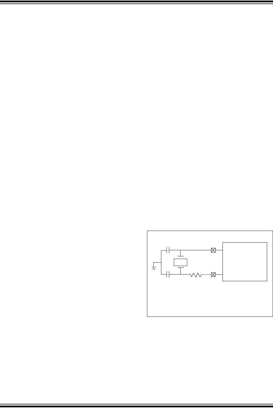
FIGURE 9-2: RECOMMENDED
COMPONENTS FOR
TIMER1 LP OSCILLATOR
RTC
SOSCI
SOSCO
R
C1
C2
dsPIC30FXXXX
32.768 kHz
XTAL
C1 = C2 = 18 pF; R = 100K