
Datasheet


Table Of Contents
- High-Performance Modified RISC CPU:
- DSP Features:
- Peripheral Features:
- Analog Features:
- Special Microcontroller Features:
- CMOS Technology:
- dsPIC30F6011A/6012A/6013A/6014A Controller Families
- Pin Diagrams
- Pin Diagrams (Continued)
- Pin Diagrams (Continued)
- Pin Diagrams (Continued)
- Table of Contents
- Most Current Data Sheet
- Errata
- Customer Notification System
- 1.0 Device Overview
- 2.0 CPU Architecture Overview
- 3.0 Memory Organization
- 3.1 Program Address Space
- FIGURE 3-1: program space memory map FOR dsPIC30F6011A/ 6013A
- FIGURE 3-2: program space memory map FOR dsPIC30F6012A/ 6014A
- TABLE 3-1: Program Space Address Construction
- FIGURE 3-3: DATA ACCESS FROM PROGRAM SPACE ADDRESS GENERATION
- 3.1.1 Data Access From Program Memory using Table Instructions
- 3.1.2 Data Access From Program Memory using Program Space Visibility
- 3.2 Data Address Space
- 3.1 Program Address Space
- 4.0 Address Generator Units
- 5.0 Interrupts
- 6.0 Flash Program Memory
- 6.1 In-Circuit Serial Programming (ICSP)
- 6.2 Run-Time Self-Programming (RTSP)
- 6.3 Table Instruction Operation Summary
- 6.4 RTSP Operation
- 6.5 Control Registers
- 6.6 Programming Operations
- 7.0 Data EEPROM Memory
- 8.0 I/O Ports
- 8.1 Parallel I/O (PIO) Ports
- 8.2 Configuring Analog Port Pins
- FIGURE 8-2: Block Diagram of a ShAred PORT Structure
- TABLE 8-1: PORTA Register MAp for dsPIC30F6013A/6014A(1)
- TABLE 8-2: PORTB Register MAp for dsPIC30F6011A/6012A/6013A/6014A(1)
- TABLE 8-3: PORTC Register MAp for dsPIC30F6011A/6012A(1)
- TABLE 8-4: PORTC Register MAp for dsPIC30F6013A/6014A(1)
- TABLE 8-5: PORTD Register MAp for dsPIC30F6011A/6012A(1)
- TABLE 8-6: PORTD Register MAp for dsPIC30F6013A/6014A(1)
- TABLE 8-7: PORTF Register MAp for dsPIC30F6011A/6012A(1)
- TABLE 8-8: PORTF Register MAp for dsPIC30F6013A/6014A(1)
- TABLE 8-9: PORTG Register MAp for dsPIC30F6011A/6012A/6013A/6014A(1)
- 8.3 Input Change Notification Module
- TABLE 8-10: Input change notification register map for dsPIC30F6011A/6012A (Bits 15-8)(1)
- TABLE 8-11: Input Change notification register map FOR dsPIC30F6011A/6012A (Bits 7-0)(1)
- TABLE 8-12: Input change notification register map for dsPIC30F6013A/6014A (Bits 15-8)(1)
- TABLE 8-13: Input Change notification register map FOR dsPIC30F6013A/6014A (Bits 7-0)(1)
- 9.0 Timer1 Module
- 10.0 Timer2/3 Module
- 11.0 Timer4/5 Module
- 12.0 Input Capture Module
- 13.0 Output Compare Module
- FIGURE 13-1: Output Compare Mode Block DiagrAm
- 13.1 Timer2 and Timer3 Selection Mode
- 13.2 Simple Output Compare Match Mode
- 13.3 Dual Output Compare Match Mode
- 13.4 Simple PWM Mode
- 13.5 Output Compare Operation During CPU Sleep Mode
- 13.6 Output Compare Operation During CPU Idle Mode
- 13.7 Output Compare Interrupts
- 14.0 SPI™ Module
- 15.0 I2C™ Module
- 15.1 Operating Function Description
- 15.2 I2C Module Addresses
- 15.3 I2C 7-bit Slave Mode Operation
- 15.4 I2C 10-bit Slave Mode Operation
- 15.5 Automatic Clock Stretch
- 15.6 Software Controlled Clock Stretching (STREN = 1)
- 15.7 Interrupts
- 15.8 Slope Control
- 15.9 IPMI Support
- 15.10 General Call Address Support
- 15.11 I2C Master Support
- 15.12 I2C Master Operation
- 15.13 I2C Module Operation During CPU Sleep and Idle Modes
- 16.0 Universal Asynchronous Receiver Transmitter (UART) Module
- 17.0 CAN Module
- 18.0 Data Converter Interface (DCI) Module
- 18.1 Module Introduction
- 18.2 Module I/O Pins
- 18.3 DCI Module Operation
- 18.3.1 MODULE ENABLE
- 18.3.2 Word Size Selection Bits
- 18.3.3 Frame SYNC GEnerator
- 18.3.4 Frame Sync Mode Control Bits
- 18.3.5 Master frame sync Operation
- 18.3.6 Slave Frame Sync Operation
- 18.3.7 Bit Clock Generator
- 18.3.8 Sample Clock Edge control Bit
- 18.3.9 Data Justification Control bit
- 18.3.10 Transmit Slot Enable Bits
- 18.3.11 Receive Slot Enable Bits
- 18.3.12 Slot Enable Bits Operation with FRame SYNC
- 18.3.13 Synchronous data transfers
- 18.3.14 Buffer Length Control
- 18.3.15 Buffer Alignment With Data Frames
- 18.3.16 Transmit STATUS BITS
- 18.3.17 RECEIVE STATUS bits
- 18.3.18 SLOT Status Bits
- 18.3.19 CSDO Mode Bit
- 18.3.20 Digital Loopback mode
- 18.3.21 Underflow Mode Control Bit
- 18.4 DCI Module Interrupts
- 18.5 DCI Module Operation During CPU Sleep and Idle Modes
- 18.6 AC-Link Mode Operation
- 18.7 I2S Mode Operation
- 19.0 12-bit Analog-to-Digital Converter (ADC) Module
- FIGURE 19-1: 12-bit ADC Functional Block Diagram
- 19.1 ADC Result Buffer
- 19.2 Conversion Operation
- 19.3 Selecting the Conversion Sequence
- 19.4 Programming the Start of Conversion Trigger
- 19.5 Aborting a Conversion
- 19.6 Selecting the ADC Conversion Clock
- 19.7 ADC Speeds
- 19.8 ADC Acquisition Requirements
- 19.9 Module Power-down Modes
- 19.10 ADC Operation During CPU Sleep and Idle Modes
- 19.11 Effects of a Reset
- 19.12 Output Formats
- 19.13 Configuring Analog Port Pins
- 19.14 Connection Considerations
- 20.0 System Integration
- 20.1 Oscillator System Overview
- 20.2 Oscillator Configurations
- 20.3 Oscillator Control Registers
- 20.4 Reset
- 20.5 Watchdog Timer (WDT)
- 20.6 Low-Voltage Detect
- 20.7 Power-Saving Modes
- 20.8 Device Configuration Registers
- 20.9 Peripheral Module Disable (PMD) Registers
- 20.10 In-Circuit Debugger
- 21.0 Instruction Set Summary
- 22.0 Development Support
- 22.1 MPLAB Integrated Development Environment Software
- 22.2 MPLAB C Compilers for Various Device Families
- 22.3 HI-TECH C for Various Device Families
- 22.4 MPASM Assembler
- 22.5 MPLINK Object Linker/ MPLIB Object Librarian
- 22.6 MPLAB Assembler, Linker and Librarian for Various Device Families
- 22.7 MPLAB SIM Software Simulator
- 22.8 MPLAB REAL ICE In-Circuit Emulator System
- 22.9 MPLAB ICD 3 In-Circuit Debugger System
- 22.10 PICkit 3 In-Circuit Debugger/ Programmer and PICkit 3 Debug Express
- 22.11 PICkit 2 Development Programmer/Debugger and PICkit 2 Debug Express
- 22.12 MPLAB PM3 Device Programmer
- 22.13 Demonstration/Development Boards, Evaluation Kits, and Starter Kits
- 23.0 Electrical Characteristics
- Absolute Maximum Ratings(†)
- 23.1 DC Characteristics
- TABLE 23-1: Operating MIPS vs. Voltage
- TABLE 23-2: Thermal Operating Conditions
- TABLE 23-3: Thermal Packaging Characteristics
- TABLE 23-4: DC Temperature and Voltage specifications
- TABLE 23-5: DC Characteristics: Operating Current (Idd)
- TABLE 23-6: DC Characteristics: Idle Current (iidle)
- TABLE 23-7: DC Characteristics: Power-Down Current (Ipd)
- TABLE 23-8: DC Characteristics: I/O Pin Input Specifications
- TABLE 23-9: DC Characteristics: I/O Pin Output Specifications
- FIGURE 23-1: Low-Voltage Detect Characteristics
- TABLE 23-10: Electrical Characteristics: LVDL
- FIGURE 23-2: Brown-out Reset Characteristics
- TABLE 23-11: Electrical Characteristics: BOR
- TABLE 23-12: DC Characteristics: Program and EEPROM
- 23.2 AC Characteristics and Timing Parameters
- TABLE 23-13: Temperature and Voltage Specifications – AC
- FIGURE 23-3: Load Conditions for Device Timing Specifications
- FIGURE 23-4: External Clock Timing
- TABLE 23-14: External Clock Timing Requirements
- TABLE 23-15: PLL Clock Timing Specifications (Vdd = 2.5 to 5.5 V)
- TABLE 23-16: PLL Jitter
- TABLE 23-17: Internal Clock Timing examples
- TABLE 23-18: AC Characteristics: Internal FRC Accuracy
- TABLE 23-19: AC Characteristics: Internal LPRC accuracy
- FIGURE 23-5: CLKOUT and I/O Timing Characteristics
- TABLE 23-20: CLKOUT and I/O Timing Requirements
- FIGURE 23-6: Reset, Watchdog Timer, Oscillator Start-up Timer and Power-up Timer Timing Characteristics
- TABLE 23-21: Reset, Watchdog Timer, Oscillator Start-up Timer, Power-up Timer and Brown-out Reset Timing Requirements
- FIGURE 23-7: band gap Start-up Time Characteristics
- TABLE 23-22: band gap Start-up Time Requirements
- FIGURE 23-8: Type A, B and C Timer External Clock Timing Characteristics
- TABLE 23-23: TYPE A TIMER (Timer1) External Clock Timing Requirements(1)
- TABLE 23-24: TYPE B TIMER (Timer2 and Timer4) External Clock Timing Requirements(1)
- TABLE 23-25: TYPE C TIMER (Timer3 and Timer5) External Clock Timing Requirements(1)
- FIGURE 23-9: INPUT CAPTURE (CAPx) TIMING Characteristics
- TABLE 23-26: Input Capture timing requirements
- FIGURE 23-10: Output Compare Module (OCx) Timing Characteristics
- TABLE 23-27: Output Compare Module timing requirements
- FIGURE 23-11: OC/PWM Module Timing Characteristics
- TABLE 23-28: Simple OC/PWM MODE Timing Requirements
- FIGURE 23-12: DCI Module (Multichannel, I2S modes) Timing Characteristics
- TABLE 23-29: DCI Module (Multichannel, I2S modes) Timing Requirements
- FIGURE 23-13: DCI Module (AC-link mode) Timing Characteristics
- TABLE 23-30: DCI Module (AC-Link Mode) Timing Requirements
- FIGURE 23-14: SPI Module Master Mode (CKE = 0) Timing Characteristics
- TABLE 23-31: SPI Master mode (cke = 0) Timing requirements
- FIGURE 23-15: SPI Module Master Mode (CKE =1) Timing Characteristics
- TABLE 23-32: SPI Module Master mode (cke = 1) Timing requirements
- FIGURE 23-16: SPI Module Slave Mode (CKE = 0) Timing Characteristics
- TABLE 23-33: SPI Module Slave mode (cke = 0) Timing requirements
- FIGURE 23-17: SPI Module Slave Mode (CKE = 1) Timing Characteristics
- TABLE 23-34: SPI Module Slave mode (cke = 1) Timing requirements
- FIGURE 23-18: I2C™ Bus Start/Stop Bits Timing Characteristics (Master mode)
- FIGURE 23-19: I2C™ Bus Data Timing Characteristics (Master mode)
- TABLE 23-35: I2C™ Bus Data Timing Requirements (Master Mode)
- FIGURE 23-20: I2C™ Bus Start/Stop Bits Timing Characteristics (slave mode)
- FIGURE 23-21: I2C™ Bus Data Timing Characteristics (slave mode)
- TABLE 23-36: I2C™ Bus Data Timing Requirements (Slave Mode)
- FIGURE 23-22: CAN Module I/O Timing Characteristics
- TABLE 23-37: CAN Module I/O Timing Requirements
- TABLE 23-38: 12-bit ADC Module Specifications
- FIGURE 23-23: 12-Bit ADC Timing Characteristics (asam = 0, ssrc = 000)
- TABLE 23-39: 12-BIT ADC TiminG rEQUIREMENTS
- 24.0 Packaging Information
- Appendix A: Revision History
- Index
- The Microchip Web Site
- Customer Change Notification Service
- Customer Support
- Reader Response
- Product Identification System
© 2011 Microchip Technology Inc. DS70143E-page 137
dsPIC30F6011A/6012A/6013A/6014A
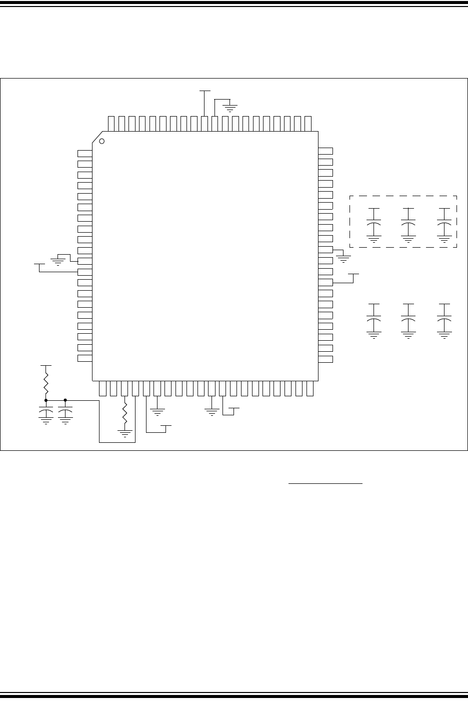
The following figure depicts the recommended circuit
for the conversion rates above 100 ksps. The
dsPIC30F6014A is shown as an example.
FIGURE 19-2: ADC VOLTAGE REFERENCE SCHEMATIC
The configuration procedures below give the required
setup values for the conversion speeds above 100
ksps.
19.7.1 200 KSPS CONFIGURATION
GUIDELINE
The following configuration items are required to
achieve a 200 ksps conversion rate.
• Comply with conditions provided in Tab l e 1 9 -2 .
• Connect external V
REF+ and VREF- pins following
the recommended circuit as shown in Figure 19-2.
• Set SSRC<2.0> = 111 in the ADCON1 register to
enable the auto convert option.
• Enable automatic sampling by setting the ASAM
control bit in the ADCON1 register.
• Write the SMPI<3.0> control bits in the ADCON2
register for the desired number of conversions
between interrupts.
• Configure the ADC clock period to be:
by writing to the ADCS<5:0> control bits in the
ADCON3 register.
• Configure the sampling time to be 1 T
AD by
writing: SAMC<4:0> = 00001.
The following figure shows the timing diagram of the
ADC running at 200 ksps. The T
AD selection in conjunc-
tion with the guidelines described above allows a con-
version speed of 200 ksps. See Example 19-1 for code
example.
72
74
73
V
DD
VSS
69
68
67
66
65
64
63
62
61
20
2
3
4
5
6
7
8
9
10
V
SS
VDD
13
14
15
16
50
49
V
DD
47
46
45
44
21
41
40
39
38
37
36
35
34
V
REF-
V
REF+
AV
DD
AVSS
27
28
29
30
V
SS
VDD
33
17
18
19
75
1
57
56
55
54
53
52
V
SS
60
59
58
43
42
76
78
77
79
22
80
dsPIC30F6014A
VDD
VDD
VDD
VDD
VDD
VDD
VDD
R2
10
C2
0.1 μF
C1
0.01 μF
R1
10
C8
1 μF
VDD
C7
0.1 μF
VDD
C6
0.01 μF
AVDD
C5
1 μF
AVDD
C4
0.1 μF
AVDD
C3
0.01 μF
See Note 1:
Note 1: Ensure adequate bypass capacitors are provided on each VDD pin.
1
(14 + 1) x 200,000
= 334 ns