
Datasheet


Table Of Contents
- High-Performance Modified RISC CPU:
- DSP Features:
- Peripheral Features:
- Analog Features:
- Special Microcontroller Features:
- CMOS Technology:
- dsPIC30F6011A/6012A/6013A/6014A Controller Families
- Pin Diagrams
- Pin Diagrams (Continued)
- Pin Diagrams (Continued)
- Pin Diagrams (Continued)
- Table of Contents
- Most Current Data Sheet
- Errata
- Customer Notification System
- 1.0 Device Overview
- 2.0 CPU Architecture Overview
- 3.0 Memory Organization
- 3.1 Program Address Space
- FIGURE 3-1: program space memory map FOR dsPIC30F6011A/ 6013A
- FIGURE 3-2: program space memory map FOR dsPIC30F6012A/ 6014A
- TABLE 3-1: Program Space Address Construction
- FIGURE 3-3: DATA ACCESS FROM PROGRAM SPACE ADDRESS GENERATION
- 3.1.1 Data Access From Program Memory using Table Instructions
- 3.1.2 Data Access From Program Memory using Program Space Visibility
- 3.2 Data Address Space
- 3.1 Program Address Space
- 4.0 Address Generator Units
- 5.0 Interrupts
- 6.0 Flash Program Memory
- 6.1 In-Circuit Serial Programming (ICSP)
- 6.2 Run-Time Self-Programming (RTSP)
- 6.3 Table Instruction Operation Summary
- 6.4 RTSP Operation
- 6.5 Control Registers
- 6.6 Programming Operations
- 7.0 Data EEPROM Memory
- 8.0 I/O Ports
- 8.1 Parallel I/O (PIO) Ports
- 8.2 Configuring Analog Port Pins
- FIGURE 8-2: Block Diagram of a ShAred PORT Structure
- TABLE 8-1: PORTA Register MAp for dsPIC30F6013A/6014A(1)
- TABLE 8-2: PORTB Register MAp for dsPIC30F6011A/6012A/6013A/6014A(1)
- TABLE 8-3: PORTC Register MAp for dsPIC30F6011A/6012A(1)
- TABLE 8-4: PORTC Register MAp for dsPIC30F6013A/6014A(1)
- TABLE 8-5: PORTD Register MAp for dsPIC30F6011A/6012A(1)
- TABLE 8-6: PORTD Register MAp for dsPIC30F6013A/6014A(1)
- TABLE 8-7: PORTF Register MAp for dsPIC30F6011A/6012A(1)
- TABLE 8-8: PORTF Register MAp for dsPIC30F6013A/6014A(1)
- TABLE 8-9: PORTG Register MAp for dsPIC30F6011A/6012A/6013A/6014A(1)
- 8.3 Input Change Notification Module
- TABLE 8-10: Input change notification register map for dsPIC30F6011A/6012A (Bits 15-8)(1)
- TABLE 8-11: Input Change notification register map FOR dsPIC30F6011A/6012A (Bits 7-0)(1)
- TABLE 8-12: Input change notification register map for dsPIC30F6013A/6014A (Bits 15-8)(1)
- TABLE 8-13: Input Change notification register map FOR dsPIC30F6013A/6014A (Bits 7-0)(1)
- 9.0 Timer1 Module
- 10.0 Timer2/3 Module
- 11.0 Timer4/5 Module
- 12.0 Input Capture Module
- 13.0 Output Compare Module
- FIGURE 13-1: Output Compare Mode Block DiagrAm
- 13.1 Timer2 and Timer3 Selection Mode
- 13.2 Simple Output Compare Match Mode
- 13.3 Dual Output Compare Match Mode
- 13.4 Simple PWM Mode
- 13.5 Output Compare Operation During CPU Sleep Mode
- 13.6 Output Compare Operation During CPU Idle Mode
- 13.7 Output Compare Interrupts
- 14.0 SPI™ Module
- 15.0 I2C™ Module
- 15.1 Operating Function Description
- 15.2 I2C Module Addresses
- 15.3 I2C 7-bit Slave Mode Operation
- 15.4 I2C 10-bit Slave Mode Operation
- 15.5 Automatic Clock Stretch
- 15.6 Software Controlled Clock Stretching (STREN = 1)
- 15.7 Interrupts
- 15.8 Slope Control
- 15.9 IPMI Support
- 15.10 General Call Address Support
- 15.11 I2C Master Support
- 15.12 I2C Master Operation
- 15.13 I2C Module Operation During CPU Sleep and Idle Modes
- 16.0 Universal Asynchronous Receiver Transmitter (UART) Module
- 17.0 CAN Module
- 18.0 Data Converter Interface (DCI) Module
- 18.1 Module Introduction
- 18.2 Module I/O Pins
- 18.3 DCI Module Operation
- 18.3.1 MODULE ENABLE
- 18.3.2 Word Size Selection Bits
- 18.3.3 Frame SYNC GEnerator
- 18.3.4 Frame Sync Mode Control Bits
- 18.3.5 Master frame sync Operation
- 18.3.6 Slave Frame Sync Operation
- 18.3.7 Bit Clock Generator
- 18.3.8 Sample Clock Edge control Bit
- 18.3.9 Data Justification Control bit
- 18.3.10 Transmit Slot Enable Bits
- 18.3.11 Receive Slot Enable Bits
- 18.3.12 Slot Enable Bits Operation with FRame SYNC
- 18.3.13 Synchronous data transfers
- 18.3.14 Buffer Length Control
- 18.3.15 Buffer Alignment With Data Frames
- 18.3.16 Transmit STATUS BITS
- 18.3.17 RECEIVE STATUS bits
- 18.3.18 SLOT Status Bits
- 18.3.19 CSDO Mode Bit
- 18.3.20 Digital Loopback mode
- 18.3.21 Underflow Mode Control Bit
- 18.4 DCI Module Interrupts
- 18.5 DCI Module Operation During CPU Sleep and Idle Modes
- 18.6 AC-Link Mode Operation
- 18.7 I2S Mode Operation
- 19.0 12-bit Analog-to-Digital Converter (ADC) Module
- FIGURE 19-1: 12-bit ADC Functional Block Diagram
- 19.1 ADC Result Buffer
- 19.2 Conversion Operation
- 19.3 Selecting the Conversion Sequence
- 19.4 Programming the Start of Conversion Trigger
- 19.5 Aborting a Conversion
- 19.6 Selecting the ADC Conversion Clock
- 19.7 ADC Speeds
- 19.8 ADC Acquisition Requirements
- 19.9 Module Power-down Modes
- 19.10 ADC Operation During CPU Sleep and Idle Modes
- 19.11 Effects of a Reset
- 19.12 Output Formats
- 19.13 Configuring Analog Port Pins
- 19.14 Connection Considerations
- 20.0 System Integration
- 20.1 Oscillator System Overview
- 20.2 Oscillator Configurations
- 20.3 Oscillator Control Registers
- 20.4 Reset
- 20.5 Watchdog Timer (WDT)
- 20.6 Low-Voltage Detect
- 20.7 Power-Saving Modes
- 20.8 Device Configuration Registers
- 20.9 Peripheral Module Disable (PMD) Registers
- 20.10 In-Circuit Debugger
- 21.0 Instruction Set Summary
- 22.0 Development Support
- 22.1 MPLAB Integrated Development Environment Software
- 22.2 MPLAB C Compilers for Various Device Families
- 22.3 HI-TECH C for Various Device Families
- 22.4 MPASM Assembler
- 22.5 MPLINK Object Linker/ MPLIB Object Librarian
- 22.6 MPLAB Assembler, Linker and Librarian for Various Device Families
- 22.7 MPLAB SIM Software Simulator
- 22.8 MPLAB REAL ICE In-Circuit Emulator System
- 22.9 MPLAB ICD 3 In-Circuit Debugger System
- 22.10 PICkit 3 In-Circuit Debugger/ Programmer and PICkit 3 Debug Express
- 22.11 PICkit 2 Development Programmer/Debugger and PICkit 2 Debug Express
- 22.12 MPLAB PM3 Device Programmer
- 22.13 Demonstration/Development Boards, Evaluation Kits, and Starter Kits
- 23.0 Electrical Characteristics
- Absolute Maximum Ratings(†)
- 23.1 DC Characteristics
- TABLE 23-1: Operating MIPS vs. Voltage
- TABLE 23-2: Thermal Operating Conditions
- TABLE 23-3: Thermal Packaging Characteristics
- TABLE 23-4: DC Temperature and Voltage specifications
- TABLE 23-5: DC Characteristics: Operating Current (Idd)
- TABLE 23-6: DC Characteristics: Idle Current (iidle)
- TABLE 23-7: DC Characteristics: Power-Down Current (Ipd)
- TABLE 23-8: DC Characteristics: I/O Pin Input Specifications
- TABLE 23-9: DC Characteristics: I/O Pin Output Specifications
- FIGURE 23-1: Low-Voltage Detect Characteristics
- TABLE 23-10: Electrical Characteristics: LVDL
- FIGURE 23-2: Brown-out Reset Characteristics
- TABLE 23-11: Electrical Characteristics: BOR
- TABLE 23-12: DC Characteristics: Program and EEPROM
- 23.2 AC Characteristics and Timing Parameters
- TABLE 23-13: Temperature and Voltage Specifications – AC
- FIGURE 23-3: Load Conditions for Device Timing Specifications
- FIGURE 23-4: External Clock Timing
- TABLE 23-14: External Clock Timing Requirements
- TABLE 23-15: PLL Clock Timing Specifications (Vdd = 2.5 to 5.5 V)
- TABLE 23-16: PLL Jitter
- TABLE 23-17: Internal Clock Timing examples
- TABLE 23-18: AC Characteristics: Internal FRC Accuracy
- TABLE 23-19: AC Characteristics: Internal LPRC accuracy
- FIGURE 23-5: CLKOUT and I/O Timing Characteristics
- TABLE 23-20: CLKOUT and I/O Timing Requirements
- FIGURE 23-6: Reset, Watchdog Timer, Oscillator Start-up Timer and Power-up Timer Timing Characteristics
- TABLE 23-21: Reset, Watchdog Timer, Oscillator Start-up Timer, Power-up Timer and Brown-out Reset Timing Requirements
- FIGURE 23-7: band gap Start-up Time Characteristics
- TABLE 23-22: band gap Start-up Time Requirements
- FIGURE 23-8: Type A, B and C Timer External Clock Timing Characteristics
- TABLE 23-23: TYPE A TIMER (Timer1) External Clock Timing Requirements(1)
- TABLE 23-24: TYPE B TIMER (Timer2 and Timer4) External Clock Timing Requirements(1)
- TABLE 23-25: TYPE C TIMER (Timer3 and Timer5) External Clock Timing Requirements(1)
- FIGURE 23-9: INPUT CAPTURE (CAPx) TIMING Characteristics
- TABLE 23-26: Input Capture timing requirements
- FIGURE 23-10: Output Compare Module (OCx) Timing Characteristics
- TABLE 23-27: Output Compare Module timing requirements
- FIGURE 23-11: OC/PWM Module Timing Characteristics
- TABLE 23-28: Simple OC/PWM MODE Timing Requirements
- FIGURE 23-12: DCI Module (Multichannel, I2S modes) Timing Characteristics
- TABLE 23-29: DCI Module (Multichannel, I2S modes) Timing Requirements
- FIGURE 23-13: DCI Module (AC-link mode) Timing Characteristics
- TABLE 23-30: DCI Module (AC-Link Mode) Timing Requirements
- FIGURE 23-14: SPI Module Master Mode (CKE = 0) Timing Characteristics
- TABLE 23-31: SPI Master mode (cke = 0) Timing requirements
- FIGURE 23-15: SPI Module Master Mode (CKE =1) Timing Characteristics
- TABLE 23-32: SPI Module Master mode (cke = 1) Timing requirements
- FIGURE 23-16: SPI Module Slave Mode (CKE = 0) Timing Characteristics
- TABLE 23-33: SPI Module Slave mode (cke = 0) Timing requirements
- FIGURE 23-17: SPI Module Slave Mode (CKE = 1) Timing Characteristics
- TABLE 23-34: SPI Module Slave mode (cke = 1) Timing requirements
- FIGURE 23-18: I2C™ Bus Start/Stop Bits Timing Characteristics (Master mode)
- FIGURE 23-19: I2C™ Bus Data Timing Characteristics (Master mode)
- TABLE 23-35: I2C™ Bus Data Timing Requirements (Master Mode)
- FIGURE 23-20: I2C™ Bus Start/Stop Bits Timing Characteristics (slave mode)
- FIGURE 23-21: I2C™ Bus Data Timing Characteristics (slave mode)
- TABLE 23-36: I2C™ Bus Data Timing Requirements (Slave Mode)
- FIGURE 23-22: CAN Module I/O Timing Characteristics
- TABLE 23-37: CAN Module I/O Timing Requirements
- TABLE 23-38: 12-bit ADC Module Specifications
- FIGURE 23-23: 12-Bit ADC Timing Characteristics (asam = 0, ssrc = 000)
- TABLE 23-39: 12-BIT ADC TiminG rEQUIREMENTS
- 24.0 Packaging Information
- Appendix A: Revision History
- Index
- The Microchip Web Site
- Customer Change Notification Service
- Customer Support
- Reader Response
- Product Identification System
© 2011 Microchip Technology Inc. DS70143E-page 107
dsPIC30F6011A/6012A/6013A/6014A
16.5.2 FRAMING ERROR (FERR)
The FERR bit (UxSTA<2>) is set if a ‘0’ is detected
instead of a Stop bit. If two Stop bits are selected, both
Stop bits must be ‘1’, otherwise FERR will be set. The
read only FERR bit is buffered along with the received
data. It is cleared on any Reset.
16.5.3 PARITY ERROR (PERR)
The PERR bit (UxSTA<3>) is set if the parity of the
received word is incorrect. This error bit is applicable
only if a Parity mode (odd or even) is selected. The
read only PERR bit is buffered along with the received
data bytes. It is cleared on any Reset.
16.5.4 IDLE STATUS
When the receiver is active (i.e., between the initial
detection of the Start bit and the completion of the Stop
bit), the RIDLE bit (UxSTA<4>) is ‘0’. Between the com-
pletion of the Stop bit and detection of the next Start bit,
the RIDLE bit is ‘1’, indicating that the UART is Idle.
16.5.5 RECEIVE BREAK
The receiver will count and expect a certain number of
bit times based on the values programmed in the
PDSEL (UxMODE<2:1>) and STSEL (UxMODE<0>)
bits.
If the break is longer than 13 bit times, the reception is
considered complete after the number of bit times
specified by PDSEL and STSEL. The URXDA bit is set,
FERR is set, zeros are loaded into the receive FIFO,
interrupts are generated if appropriate and the RIDLE
bit is set.
When the module receives a long break signal and the
receiver has detected the Start bit, the data bits and the
invalid Stop bit (which sets the FERR), the receiver
must wait for a valid Stop bit before looking for the next
Start bit. It cannot assume that the break condition on
the line is the next Start bit.
Break is regarded as a character containing all ‘0’s with
the FERR bit set. The break character is loaded into the
buffer. No further reception can occur until a Stop bit is
received. Note that RIDLE goes high when the Stop bit
has not yet been received.
16.6 Address Detect Mode
Setting the ADDEN bit (UxSTA<5>) enables this spe-
cial mode in which a 9th bit (URX8) value of ‘1’ identi-
fies the received word as an address, rather than data.
This mode is only applicable for 9-bit data communica-
tion. The URXISEL control bit does not have any
impact on interrupt generation in this mode since an
interrupt (if enabled) will be generated every time the
received word has the 9th bit set.
16.7 Loopback Mode
Setting the LPBACK bit enables this special mode in
which the UxTX pin is internally connected to the UxRX
pin. When configured for the Loopback mode, the
UxRX pin is disconnected from the internal UART
receive logic. However, the UxTX pin still functions as
in a normal operation.
To select this mode:
1. Configure UART for desired mode of operation.
2. Set LPBACK = 1 to enable Loopback mode.
3. Enable transmission as defined in Section 16.3
“Transmitting Data”.
16.8 Baud Rate Generator
The UART has a 16-bit Baud Rate Generator to allow
maximum flexibility in baud rate generation. The Baud
Rate Generator register (UxBRG) is readable and
writable. The baud rate is computed as shown in
Equation 16-1:
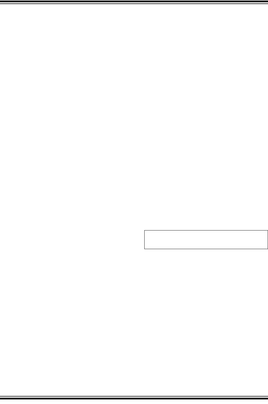
EQUATION 16-1: BAUD RATE
Where:
BRG = 16-bit value held in UxBRG register
(0 through 65535)
F
CY = Instruction Clock Rate (1/TCY)
Therefore, the maximum baud rate possible is:
F
CY/16 (if BRG = 0),
and the minimum baud rate possible is:
F
CY/(16 * 65536).
With a full 16-bit Baud Rate Generator at 30 MIPS
operation, the minimum baud rate achievable is
28.5 bps.
Baud Rate = FCY/(16 * (BRG + 1))