
Datasheet


2010 Microchip Technology Inc. DS70138G-page 195
dsPIC30F3014/4013
FIGURE 23-14: SPI MODULE MASTER MODE (CKE = 0) TIMING CHARACTERISTICS
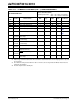
TABLE 23-29: DCI MODULE (AC-LINK MODE) TIMING REQUIREMENTS
AC CHARACTERISTICS
Standard Operating Conditions: 2.5V to 5.5V
(unless otherwise stated)
Operating temperature -40°C T
A +85°C for Industrial
-40°C T
A +125°C for Extended
Param
No.
Symbol Characteristic
(1,2)
Min Typ
(3)
Max Units Conditions
CS60 T
BCLKL BIT_CLK Low Time 36 40.7 45 ns
CS61 T
BCLKH BIT_CLK High Time 36 40.7 45 ns
CS62 T
BCLK BIT_CLK Period — 81.4 — ns Bit clock is input
CS65 T
SACL Input Setup Time to
Falling Edge of BIT_CLK
——10ns
CS66 T
HACL Input Hold Time from
Falling Edge of BIT_CLK
——10ns
CS70 T
SYNCLO SYNC Data Output Low Time — 19.5 — s Note 1
CS71 T
SYNCHI SYNC Data Output High Time — 1.3 — s Note 1
CS72 T
SYNC SYNC Data Output Period — 20.8 — s Note 1
CS75 T
RACL Rise Time, SYNC, SDATA_OUT — 10 25 ns CLOAD = 50 pF, VDD = 5V
CS76 TFACL Fall Time, SYNC, SDATA_OUT — 10 25 ns CLOAD = 50 pF, VDD = 5V
CS80 T
OVDACL Output Valid Delay from Rising
Edge of BIT_CLK
——15ns
Note 1: These parameters are characterized but not tested in manufacturing.
2: These values assume BIT_CLK frequency is 12.288 MHz.
3: Data in “Typ” column is at 5V, 25°C unless otherwise stated. Parameters are for design guidance only and
are not tested.
SCKx
(CKP = 0)
SCKx
(CKP = 1)
SDOx
SDIx
SP11 SP10
SP40
SP41
SP21
SP20
SP35
SP20
SP21
MSb LSb
Bit 14 - - - - - -1
MSb In
LSb In
Bit 14 - - - -1
SP30
SP31
Note: Refer to Figure 23-3 for load conditions.