
Datasheet


2010 Microchip Technology Inc. DS70138G-page 161
dsPIC30F3014/4013
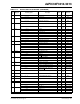
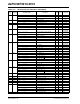
Wb Base W register {W0..W15}
Wd Destination W register { Wd, [Wd], [Wd++], [Wd--], [++Wd], [--Wd] }
Wdo Destination W register
{ Wnd, [Wnd], [Wnd++], [Wnd--], [++Wnd], [--Wnd], [Wnd+Wb] }
Wm,Wn Dividend, Divisor Working register pair (direct addressing)
Wm*Wm Multiplicand and Multiplier working register pair for Square instructions
{W4*W4,W5*W5,W6*W6,W7*W7}
Wm*Wn Multiplicand and Multiplier working register pair for DSP instructions
{W4*W5,W4*W6,W4*W7,W5*W6,W5*W7,W6*W7}
Wn One of 16 working registers {W0..W15}
Wnd One of 16 destination working registers {W0..W15}
Wns One of 16 source working registers {W0..W15}
WREG W0 (working register used in file register instructions)
Ws Source W register { Ws, [Ws], [Ws++], [Ws--], [++Ws], [--Ws] }
Wso Source W register
{ Wns, [Wns], [Wns++], [Wns--], [++Wns], [--Wns], [Wns+Wb] }
Wx X data space prefetch address register for DSP instructions
{[W8]+=6, [W8]+=4, [W8]+=2, [W8], [W8]-=6, [W8]-=4, [W8]-=2,
[W9]+=6, [W9]+=4, [W9]+=2, [W9], [W9]-=6, [W9]-=4, [W9]-=2,
[W9+W12],none}
Wxd X data space prefetch destination register for DSP instructions {W4..W7}
Wy Y data space prefetch address register for DSP instructions
{[W10]+=6, [W10]+=4, [W10]+=2, [W10], [W10]-=6, [W10]-=4, [W10]-=2,
[W11]+=6, [W11]+=4, [W11]+=2, [W11], [W11]-=6, [W11]-=4, [W11]-=2,
[W11+W12], none}
Wyd Y data space prefetch destination register for DSP instructions {W4..W7}
TABLE 21-1: SYMBOLS USED IN OPCODE DESCRIPTIONS (CONTINUED)
Field Description