
Datasheet


dsPIC30F4011/4012
DS70135G-page 218 © 2010 Microchip Technology Inc.
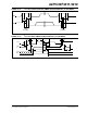
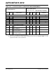
TABLE 24-40: 10-BIT HIGH-SPEED A/D CONVERSION TIMING REQUIREMENTS
AC CHARACTERISTICS
Standard Operating Conditions: 2.5V to 5.5V
(unless otherwise stated)
Operating temperature -40°C ≤ TA ≤ +85°C for Industrial
-40°C ≤ TA ≤ +125°C for Extended
Param
No.
Symbol Characteristic Min. Typ Max. Units Conditions
Clock Parameters
AD50 T
AD A/D Clock Period — 84 — ns See Table 20-2
(1)
AD51 tRC A/D Internal RC Oscillator Period 700 900 1100 ns
Conversion Rate
AD55 t
CONV Conversion Time — 12 TAD ——
AD56 FCNV Throughput Rate — 1.0 — Msps See Table 20-2
(1)
AD57 TSAMP Sample Time — 1 TAD — — See Table 20-2
(1)
Timing Parameters
AD60 tPCS Conversion Start from Sample
Trigger
— 1.0 TAD ——
AD61 t
PSS Sample Start from Setting
Sample (SAMP) Bit
0.5 TAD — 1.5 TAD —
AD62 tCSS Conversion Completion to
Sample Start (ASAM = 1)
— 0.5 TAD ——
AD63 tDPU
(2)
Time to Stabilize Analog Stage
from A/D Off to A/D On
——20μs
Note 1: Because the sample caps will eventually lose charge, clock rates below 10 kHz can affect linearity
performance, especially at elevated temperatures.
2: tDPU is the time required for the ADC module to stabilize when it is turned on (ADCON1<ADON> = 1). Dur-
ing this time the ADC result is indeterminate.