
Datasheet


dsPIC30F4011/4012
DS70135G-page 146 © 2010 Microchip Technology Inc.
20.8 A/D Acquisition Requirements
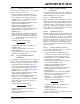
The analog input model of the 10-bit ADC is shown in
Figure 20-3. The total sampling time for the ADC is a
function of the internal amplifier settling time, device
V
DD and the holding capacitor charge time.
For the ADC to meet its specified accuracy, the charge
holding capacitor (C
HOLD) must be allowed to fully
charge to the voltage level on the analog input pin. The
source impedance (R
S), the interconnect impedance
(RIC) and the internal sampling switch (RSS) impedance
combine to directly affect the time required to charge the
capacitor C
HOLD. The combined impedance of the ana-
log sources must therefore be small enough to fully
charge the holding capacitor within the chosen sample
time. To minimize the effects of pin leakage currents on
the accuracy of the ADC, the maximum recommended
source impedance, R
S, is 5 kΩ. After the analog input
channel is selected (changed), this sampling function
must be completed prior to starting the conversion. The
internal holding capacitor will be in a discharged state
prior to each sample operation.
The user must allow at least 1 T
AD period of sampling
time, TSAMP, between conversions to allow each sam-
ple to be acquired. This sample time may be controlled
manually in software by setting/clearing the SAMP bit,
or it may be automatically controlled by the ADC. In an
automatic configuration, the user must allow enough
time between conversion triggers so that the minimum
sample time can be satisfied. Refer to Section 24.0
“Electrical Characteristics” for T
AD and sample time
requirements.
FIGURE 20-3: A/D CONVERTER ANALOG INPUT MODEL
CPIN
VA
Rs
ANx
V
T = 0.6V
V
T = 0.6V
I
LEAKAGE
RIC ≤ 250Ω
Sampling
Switch
R
SS
CHOLD
= DAC Capacitance
V
SS
VDD
= 4.4 pF
±500 nA
Legend: CPIN
VT
I leakage
R
IC
RSS
CHOLD
= Input Capacitance
= Threshold Voltage
= Leakage Current at the pin due to
= Interconnect Resistance
= Sampling Switch Resistance
= Sample/Hold Capacitance (from DAC)
various junctions
Note: CPIN value depends on device package and is not tested. Effect of CPIN negligible if Rs ≤ 5 kΩ.
RSS ≤ 3 kΩ