
Datasheet


dsPIC30F4011/4012
DS70135G-page 102 © 2010 Microchip Technology Inc.
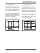
15.5 PWM Duty Cycle Comparison
Units
There are three 16-bit Special Function Registers
(PDC1, PDC2 and PDC3) used to specify duty cycle
values for the PWM module.
The value in each duty cycle register determines the
amount of time that the PWM output is in the active
state. The duty cycle registers are 16-bits wide. The
LSb of a duty cycle register determines whether the
PWM edge occurs in the beginning. Thus, the PWM
resolution is effectively doubled.
15.5.1 DUTY CYCLE REGISTER BUFFERS
The three PWM duty cycle registers are double-
buffered to allow glitchless updates of the PWM
outputs. For each duty cycle, there is a duty cycle
register that is accessible by the user and a second
duty cycle register that holds the actual compare value
used in the present PWM period.
For edge-aligned PWM output, a new duty cycle value
will be updated whenever a match with the PTPER reg-
ister occurs and PTMR is reset. The contents of the
duty cycle buffers are automatically loaded into the
duty cycle registers when the PWM time base is dis-
abled (PTEN = 0) and the UDIS bit is cleared in
PWMCON2.
When the PWM time base is in the Continuous Up/
Down Count mode, new duty cycle values are updated
when the value of the PTMR register is zero and the
PWM time base begins to count upwards. The contents
of the duty cycle buffers are automatically loaded into
the duty cycle registers when the PWM time base is
disabled (PTEN = 0).
When the PWM time base is in the Continuous Up/
Down Count mode with double updates, new duty cycle
values are updated when the value of the PTMR regis-
ter is zero, and when the value of the PTMR register
matches the value in the PTPER register. The contents
of the duty cycle buffers are automatically loaded into
the duty cycle registers when the PWM time base is
disabled (PTEN = 0).
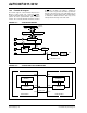
15.6 Complementary PWM Operation
In the Complementary mode of operation, each pair of
PWM outputs is obtained by a complementary PWM
signal. A dead time may be optionally inserted during
device switching when both outputs are inactive for
a short period (refer to Section 15.7 “Dead-Time
Generators”).
In Complementary mode, the duty cycle comparison
units are assigned to the PWM outputs as follows:
• PDC1 register controls PWM1H/PWM1L outputs
• PDC2 register controls PWM2H/PWM2L outputs
• PDC3 register controls PWM3H/PWM3L outputs
The Complementary mode is selected for each PWM
I/O pin pair by clearing the appropriate PTMODx bit in
the PWMCON1 SFR. The PWM I/O pins are set to
Complementary mode by default upon a device Reset.
15.7 Dead-Time Generators
Dead-time generation may be provided when any of
the PWM I/O pin pairs are operating in the
Complementary Output mode. The PWM outputs use
push-pull drive circuits. Due to the inability of the power
output devices to switch instantaneously, some amount
of time must be provided between the turn-off event
of one PWM output in a complementary pair and the
turn-on event of the other transistor.
The PWM module allows two different dead times to be
programmed. These two dead times may be used in
one of two methods described below to increase user
flexibility:
• The PWM output signals can be optimized for
different turn-off times in the high side and low
side transistors in a complementary pair of tran-
sistors. The first dead time is inserted between
the turn-off event of the lower transistor of the
complementary pair and the turn-on event of the
upper transistor. The second dead time is inserted
between the turn-off event of the upper transistor
and the turn-on event of the lower transistor.
• The two dead times can be assigned to individual
PWM I/O pin pairs. This operating mode allows
the PWM module to drive different transistor/load
combinations with each complementary PWM I/O
pin pair.