
Datasheet


dsPIC30F4011/4012
DS70135G-page 144 © 2010 Microchip Technology Inc.
The configuration guidelines give the required setup
values for the conversion speeds above 500 ksps,
since they require external VREF pins usage and there
are some differences in the configuration procedure.
Configuration details that are not critical to the
conversion speed have been omitted.
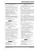
Figure 20-2 illustrates the recommended circuit for the
conversion rates above 500 ksps.
FIGURE 20-2: A/D CONVERTER VOLTAGE REFERENCE SCHEMATIC
20.7.1 1 Msps CONFIGURATION
GUIDELINE
The configuration for 1 Msps operation is dependent on
whether a single input pin is to be sampled or whether
multiple pins are to be sampled.
20.7.1.1 Single Analog Input
For conversions at 1 Msps for a single analog input, at
least two sample and hold channels must be enabled.
The analog input multiplexer must be configured so
that the same input pin is connected to both sample
and hold channels. The A/D converts the value held on
one S&H channel while the second S&H channel
acquires a new input sample.
20.7.1.2 Multiple Analog Inputs
The ADC can also be used to sample multiple analog
inputs using multiple sample and hold channels. In this
case, the total 1 Msps conversion rate is divided among
the different input signals. For example, four inputs can
be sampled at a rate of 250 ksps for each signal, or two
inputs could be sampled at a rate of 500 ksps for each
signal. Sequential sampling must be used in this
configuration to allow adequate sampling time on each
input.
V
REF
-
V
REF
+
V
DD
V
DD
VDD
V
DD
V
DD
VDD
R1
10
VDD VDD
11
1
22
12
44
33
23
34
VDD
VSS
AVDD
AVSS
VDD
VSS
VDD
VSS
dsPIC30F4011
C1
0.01 μF
C2
0.1 μF
R2
10
C8
1 μF
C7
0.1 μF
C6
0.01 μF
VDD VDD VDD
C5
1 μF
C4
0.1 μF
C3
0.01 μF