
Datasheet


2010 Microchip Technology Inc. DS70138G-page 193
dsPIC30F3014/4013
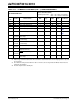
TABLE 23-28: DCI MODULE (MULTICHANNEL, I
2
S MODES) TIMING REQUIREMENTS
AC CHARACTERISTICS
Standard Operating Conditions: 2.5V to 5.5V
(unless otherwise stated)
Operating temperature -40°C T
A +85°C for Industrial
-40°C T
A +125°C for Extended
Param
No.
Symbol Characteristic
(1)
Min Typ
(2)
Max Units Conditions
CS10 Tc
SCKL CSCK Input Low Time
(CSCK pin is an input)
TCY/2 + 20 — — ns
CSCK Output Low Time
(CSCK pin is an output)
(3)
30 — — ns
CS11 Tc
SCKH CSCK Input High Time
(CSCK pin is an input)
TCY/2 + 20 — — ns
CSCK Output High Time
(CSCK pin is an output)
(3)
30 — — ns
CS20 Tc
SCKF CSCK Output Fall Time
(CSCK pin is an output)
(4)
—1025ns
CS21 Tc
SCKR CSCK Output Rise Time
(CSCK pin is an output)
(4)
—1025ns
CS30 Tc
SDOF CSDO Data Output Fall Time
(4)
—1025ns
CS31 TcSDOR CSDO Data Output Rise Time
(4)
—1025ns
CS35 T
DV Clock Edge to CSDO Data Valid — — 10 ns
CS36 TDIV Clock Edge to CSDO Tri-Stated 10 — 20 ns
CS40 TCSDI Setup Time of CSDI Data Input
to CSCK Edge (CSCK pin is
input or output)
20 — — ns
CS41 THCSDI Hold Time of CSDI Data Input to
CSCK Edge (CSCK pin is input
or output)
20 — — ns
CS50 TcoFSF COFS Fall Time
(COFS pin is output)
—1025nsNote 1
CS51 Tco
FSR COFS Rise Time
(COFS pin is output)
—1025nsNote 1
CS55 Tsco
FS Setup Time of COFS Data Input
to CSCK edge (COFS pin is
input)
20 — — ns
CS56 T
HCOFS Hold Time of COFS Data Input to
CSCK Edge (COFS pin is input)
20 — — ns
CS57 T
PCSCK CSCK Clock Period 100 — — ns
Note 1: These parameters are characterized but not tested in manufacturing.
2: Data in “Typ” column is at 5V, 25°C unless otherwise stated. Parameters are for design guidance only and
are not tested.
3: The minimum clock period for CSCK is 100 ns. Therefore, the clock generated in Master mode must not
violate this specification.
4: Assumes 50 pF load on all DCI pins.