
Datasheet


dsPIC30F1010/202X
DS70178C-page 264 Preliminary © 2006 Microchip Technology Inc.
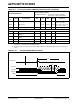
FIGURE 21-20: A/D CONVERSION TIMING PER INPUT
AD24 EOFF Offset Error — ±0.75 <±2.0 LSb VINL = AVSS = VSS = 0V,
AV
DD = VDD = 5V
AD24A EOFF Offset Error — ±0.75 <±2.0 LSb VINL = AVSS = VSS = 0V,
AV
DD = VDD = 3.3V
AD25 — Monotonicity
(2)
— — — — Guaranteed
Dynamic Performance
AD30 THD Total Harmonic Distortion -77 -73 -68 dB —
AD31 SINAD Signal to Noise and
Distortion
—58 —dB —
AD32 SFDR Spurious Free Dynamic
Range
—-73—dB —
AD33 F
NYQ Input Signal Bandwidth — — 0.5 MHz —
AD34 ENOB Effective Number of Bits — 9.4 — bits —
TABLE 21-33: 10-BIT HIGH-SPEED A/D MODULE SPECIFICATIONS (CONTINUED)
AC CHARACTERISTICS
Standard Operating Conditions: 3.3V and 5.0V (±10%)
(unless otherwise stated)
Operating temperature -40°C ≤ TA ≤ +85°C for Industrial
-40°C ≤ T
A ≤ +125°C for Extended
Param
No.
Symbol Characteristic Min. Typ Max. Units Conditions
Note 1: Because the sample caps will eventually lose charge, clock rates below 10 kHz can affect linearity
performance, especially at elevated temperatures.
2: The A/D conversion result never decreases with an increase in the input voltage, and has no missing
codes.
TAD
A/D Data
ADBUFxx
90 210
Old Data New Data
CONV
A/D Clock
Trigger Pulse
Tconv