
Datasheet


© 2006 Microchip Technology Inc. Preliminary DS70178C-page 263
dsPIC30F1010/202X
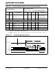
TABLE 21-33: 10-BIT HIGH-SPEED A/D MODULE SPECIFICATIONS
AC CHARACTERISTICS
Standard Operating Conditions: 3.3V and 5.0V (±10%)
(unless otherwise stated)
Operating temperature -40°C ≤ TA ≤ +85°C for Industrial
-40°C ≤ T
A ≤ +125°C for Extended
Param
No.
Symbol Characteristic Min. Typ Max. Units Conditions
Device Supply
AD01 AV
DD Module VDD Supply Greater of
V
DD – 0.3
or 2.7
Lesser of
VDD + 0.3
or 5.5
V—
AD02 AV
SS Module VSS Supply Vss – 0.3 VSS + 0.3 V —
Analog Input
AD10 V
INH-VINL Full-Scale Input Span VSS VDD V—
AD11 VIN Absolute Input Voltage AVSS – 0.3 AVDD + 0.3 V —
AD12 — Leakage Current — ±0.001 ±0.244 μAV
INL = AVSS = 0V,
AV
DD = 5V
Source Impedance = 1 kΩ
AD13 — Leakage Current — ±0.001 ±0.244 μAV
INL = AVSS = 0V,
AV
DD = 3.3V
Source Impedance = 1 kΩ
AD17 R
IN Recommended Impedance
Of Analog Voltage Source
—1KΩ —
DC Accuracy
AD20 Nr Resolution 10 data bits bits —
AD21 INL Integral Nonlinearity — ±0.5 < ±1 LSb VINL = AVSS = 0V
AV
DD = 5V
AD21A INL Integral Nonlinearity — ±0.5 < ±1 LSb VINL = AVSS = 0V
AV
DD = 3.3V
AD22 DNL Differential Nonlinearity — ±0.5 < ±1 LSb V
INL = AVSS = 0V
AV
DD = 5V
AD22A DNL Differential Nonlinearity — ±0.5 < ±1 LSb VINL = AVSS = 0V
AV
DD = 3.3V
AD23 GERR Gain Error — ±0.75 <±4.0 LSb VINL = AVSS = 0V
AV
DD = 5V
AD23A G
ERR Gain Error — ±0.75 <±3.0 LSb VINL = AVSS = 0V
AV
DD = 3.3V
Note 1: Because the sample caps will eventually lose charge, clock rates below 10 kHz can affect linearity
performance, especially at elevated temperatures.
2: The A/D conversion result never decreases with an increase in the input voltage, and has no missing
codes.