
Datasheet


© 2006 Microchip Technology Inc. Preliminary DS70178C-page 261
dsPIC30F1010/202X
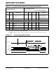
FIGURE 21-18: I
2
C™ BUS START/STOP BITS TIMING CHARACTERISTICS (SLAVE MODE)
FIGURE 21-19: I
2
C™ BUS DATA TIMING CHARACTERISTICS (SLAVE MODE)
IM50 CB Bus Capacitive Loading — 400 pF
TABLE 21-31: I
2
C™ BUS DATA TIMING REQUIREMENTS (MASTER MODE) (CONTINUED)
AC CHARACTERISTICS
Standard Operating Conditions: 3.3V and 5.0V (±10%)
(unless otherwise stated)
Operating temperature -40°C ≤ TA ≤ +85°C for Industrial
-40°C ≤ T
A ≤ +125°C for Extended
Param
No.
Symbol Characteristic Min
(1)
Max Units Conditions
Legend: TBD = To Be Determined
Note 1: BRG is the value of the I
2
C™ Baud Rate Generator. Refer to the “Inter-Integrated Circuit™ (I
2
C)”
section in the “dsPIC30F Family Reference Manual” (DS70046).
2: Maximum pin capacitance = 10 pF for all I
2
C pins (for 1 MHz mode only).
IS31
IS34
SCL
SDA
Start
Condition
Stop
Condition
IS30
IS33
IS30
IS31 IS33
IS11
IS10
IS20
IS26
IS25
IS40
IS40
IS45
IS21
SCL
SDA
In
SDA
Out