
Datasheet


dsPIC30F1010/202X
DS70178C-page 258 Preliminary © 2006 Microchip Technology Inc.
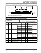
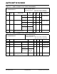
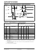
TABLE 21-30: SPI MODULE SLAVE MODE (CKE = 1) TIMING REQUIREMENTS
AC CHARACTERISTICS
Standard Operating Conditions: 3.3V and 5.0V (±10%)
(unless otherwise stated)
Operating temperature -40°C ≤ TA ≤ +85°C for Industrial
-40°C ≤ T
A ≤ +125°C for Extended
Param
No.
Symbol Characteristic
(1)
Min Typ
(2)
Max Units Conditions
SP70
TscL
SCK
X Input Low Time 30 — — ns —
SP71 TscH SCKX Input High Time 30 — — ns —
SP72 TscF SCKX Input Fall Time
(3)
—1025ns —
SP73 TscR SCK
X Input Rise Time
(3)
—1025ns —
SP30 TdoF SDOX Data Output Fall Time
(3)
— — — ns See parameter D032
SP31 TdoR SDOX Data Output Rise Time
(3)
— — — ns See parameter D031
SP35 TscH2doV,
TscL2doV
SDO
X Data Output Valid after
SCK
X Edge
——30ns —
SP40 TdiV2scH,
TdiV2scL
Setup Time of SDIX Data Input
to SCK
X Edge
20 — — ns —
SP41 TscH2diL,
TscL 2diL
Hold Time of SDIX Data Input
to SCK
X Edge
20 — — ns —
SP50 TssL2scH,
TssL2scL
SS
X↓ to SCKX↓ or SCKX↑ input 120 — — ns —
SP51 TssH2doZ SS↑ to SDOX Output
High-impedance
(4)
10 — 50 ns —
SP52 TscH2ssH
TscL2ssH
SS
X↑ after SCKX Edge 1.5 TCY
+ 40
——ns —
SP60 TssL2doV SDO
X Data Output Valid after
SS
X Edge
——50ns —
Note 1: These parameters are characterized but not tested in manufacturing.
2: Data in “Typ” column is at 5V, 25°C unless otherwise stated. Parameters are for design guidance only and
are not tested.
3: The minimum clock period for SCK is 100 ns. Therefore, the clock generated in Master mode must not
violate this specification.
4: Assumes 50 pF load on all SPI pins.