
Datasheet


© 2006 Microchip Technology Inc. Preliminary DS70178C-page 251
dsPIC30F1010/202X
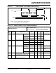
FIGURE 21-7: INPUT CAPTURE (CAPx) TIMING CHARACTERISTICS
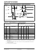
FIGURE 21-8: OUTPUT COMPARE MODULE (OCx) TIMING CHARACTERISTICS
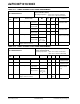
TABLE 21-23: INPUT CAPTURE TIMING REQUIREMENTS
AC CHARACTERISTICS
Standard Operating Conditions: 3.3V and 5.0V (±10%)
(unless otherwise stated)
Operating temperature -40°C ≤ TA ≤ +85°C for Industrial
-40°C ≤ T
A ≤ +125°C for Extended
Param
No.
Symbol Characteristic
(1)
Min Max Units Conditions
IC10 TccL ICx Input Low Time No Prescaler 0.5 T
CY + 20 — ns
With Prescaler 10 — ns
IC11 TccH ICx Input High Time No Prescaler 0.5 TCY + 20 — ns
With Prescaler 10 — ns
IC15 TccP ICx Input Period (2 T
CY + 40) / N — ns N = prescale
value (1, 4, 16)
Note 1: These parameters are characterized but not tested in manufacturing.
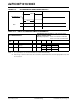
TABLE 21-24: OUTPUT COMPARE MODULE TIMING REQUIREMENTS
AC CHARACTERISTICS
Standard Operating Conditions: 3.3V and 5.0V (±10%)
(unless otherwise stated)
Operating temperature -40°C ≤ TA ≤ +85°C for Industrial
-40°C ≤ T
A ≤ +125°C for Extended
Param
No.
Symbol Characteristic
(1)
Min Typ
(2)
Max Units Conditions
OC10 TccF OCx Output Fall Time — — — ns See parameter D032
OC11 TccR OCx Output Rise Time — — — ns See parameter D031
Note 1: These parameters are characterized but not tested in manufacturing.
2: Data in “Typ” column is at 5V, 25°C unless otherwise stated. Parameters are for design guidance only and
are not tested.
ICX
IC10 IC11
IC15
Note: Refer to Figure 21-1 for load conditions.
OCx
OC11
OC10
(Output Compare
Note: Refer to Figure 21-1 for load conditions.
or PWM Mode)