
Datasheet


dsPIC30F1010/202X
DS70178C-page 242 Preliminary © 2006 Microchip Technology Inc.
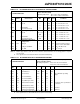
TABLE 21-13: PLL CLOCK TIMING SPECIFICATIONS (VDD = 3.0 AND 5.0V )
AC CHARACTERISTICS
Standard Operating Conditions: 3.3V and 5.0V (±10%)
(unless otherwise stated)
Operating temperature -40°C ≤ TA ≤ +85°C for Industrial
-40°C ≤ T
A ≤ +125°C for Extended
Param
No.
Symbol Characteristic
(1)
Min Typ
(2)
Max Units Conditions
OS50 FPLLI PLL Input Frequency Range
(2)
6 — 15 MHz EC, HS modes with PLL
x32
OS51 FSYS On-chip PLL Output
(2)
192 — 480 MHz EC, HS modes with PLL
x32
OS52 TLOC PLL Start-up Time (Lock Time) — 20 50 μs
OS53 D
CLK CLKO Stability (Jitter) — — 1 % Measured over 100 ms
period
Note 1: These parameters are characterized but not tested in manufacturing.
2: Data in “Typ” column is at 5V, 25°C unless otherwise stated. Parameters are for design guidance only and
are not tested.
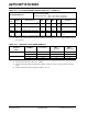
TABLE 21-14: INTERNAL CLOCK TIMING EXAMPLES
Clock
Oscillator
Mode
F
IN (MHz)
(1)
TCY (μsec)
(2)
MIPS
(3)
w/o PLL
MIPS
(4)
w/PLL x32
EC 10 0.2 5.0 20
15 0.133 7.5 30
HS 10 0.2 5.0 20
15 0.133 7.5 30
Note 1: Assumption: Oscillator Postscaler is divide by 1.
2: Instruction Execution Cycle Time: T
CY = 1/MIPS.
3: Instruction Execution Frequency without PLL: MIPS = F
IN/2 (since there are 2 Q clocks per instruction
cycle).
4: Instruction Execution Frequency with PLL: MIPS = (F
IN * 2).