
Datasheet


© 2006 Microchip Technology Inc. Preliminary DS70178C-page 241
dsPIC30F1010/202X
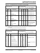
TABLE 21-12: EXTERNAL CLOCK TIMING REQUIREMENTS
AC CHARACTERISTICS
Standard Operating Conditions: 3.3V and 5.0V (±10%)
(unless otherwise stated)
Operating temperature -40°C ≤ TA ≤ +85°C for Industrial
-40°C ≤ T
A ≤ +125°C for Extended
Param
No.
Symbol Characteristic Min Typ
(1)
Max Units Conditions
OS10 F
IN External CLKI Frequency
(2)
(External clocks allowed only
in EC mode)
6
6
—
—
15.00
15.00
MHz
MHz
EC
EC with 32x PLL
Oscillator Frequency
(2)
6
6
—
—
15.00
15.00
MHz
MHz
HS
FRC internal
OS20 T
OSC TOSC = 1/FOSC
(3)
16.5 — DC ns
OS25 T
CY Instruction Cycle Time
(2)(4)
33 — DC ns
OS30 TosL,
TosH
External Clock
(2)
in (OSC1)
High or Low Time
.45 x
T
OSC
——nsEC
OS31 TosR,
TosF
External Clock
(2)
in (OSC1)
Rise or Fall Time
— — 20 ns EC
OS40 TckR CLKO Rise Time
(2)(5)
— 6 10 ns
OS41 TckF CLKO Fall Time
(2)(5)
— 6 10 ns
Note 1: Data in “Typ” column is at 5V, 25°C unless otherwise stated. Parameters are for design guidance only and
are not tested.
2: These parameters are characterized but not tested in manufacturing.
3: The oscillator frequency (F
OSC) is equal to FIN when the PLL is disabled. FOSC is equal to 4 x FIN when
the PLL is enabled.
4: Instruction cycle period (T
CY) equals two times the input oscillator time base period. All specified values
are based on characterization data for that particular oscillator type under standard operating conditions
with the device executing code. Exceeding these specified limits may result in an unstable oscillator
operation and/or higher than expected current consumption. All devices are tested to operate at “Min.”
values with an external clock applied to the OSC1/CLK1 pin. When an external clock input is used, the
“Max.” cycle time limit is “DC” (no clock) for all devices.
5: Measurements are taken in EC mode. The CLKO signal is measured on the OSC2 pin.