
Datasheet


dsPIC30F1010/202X
DS70178C-page 238 Preliminary © 2006 Microchip Technology Inc.
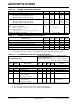
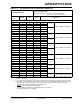
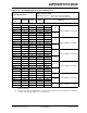
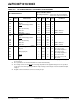
TABLE 21-8: DC CHARACTERISTICS: I/O PIN INPUT SPECIFICATIONS
DC CHARACTERISTICS
Standard Operating Conditions: 3.3V and 5.0V (±10%)
(unless otherwise stated)
Operating temperature -40°C ≤ TA ≤ +85°C for Industrial
-40°C ≤ T
A ≤ +125°C for Extended
Param
No.
Symbol Characteristic Min Typ
(1)
Max Units Conditions
V
IL
Input Low Voltage
(2)
DI10 I/O pins:
with Schmitt Trigger buffer V
SS —0.2VDD V
DI15 MCLR
VSS —0.2VDD V
DI16 OSC1 (in HS mode) VSS —0.2VDD V
DI18 SDA, SCL VSS —0.3VDD V SMbus disabled
DI19 SDA, SCL V
SS —0.2VDD V SMbus enabled
VIH Input High Voltage
(2)
DI20 I/O pins:
with Schmitt Trigger buffer 0.8 V
DD —VDD V
DI25 MCLR 0.8 VDD —VDD V
DI26 OSC1 (in HS mode) 0.7 VDD —VDD V
DI28 SDA, SCL 0.7 V
DD —VDD V SMbus disabled
DI29 SDA, SCL 0.8 VDD —VDD V SMbus enabled
IIL Input Leakage Current
(2)(3)(4)
DI50 I/O ports — 0.01 ±1 μAVSS ≤ VPIN ≤ VDD,
Pin at high-impedance
DI51 Analog input pins — 0.50 — μAV
SS ≤ VPIN ≤ VDD,
Pin at high-impedance
DI55 MCLR
—0.05±5 μAVSS ≤ VPIN ≤ VDD
DI56 OSC1 — 0.05 ±5 μAVSS ≤ VPIN ≤ VDD, HS
Osc mode
Note 1: Data in “Typ” column is at 5V, 25°C unless otherwise stated. Parameters are for design guidance only and
are not tested.
2: These parameters are characterized but not tested in manufacturing.
3: The leakage current on the MCLR pin is strongly dependent on the applied voltage level. The specified
levels represent normal operating conditions. Higher leakage current may be measured at different input
voltages.
4: Negative current is defined as current sourced by the pin.