
Datasheet


dsPIC30F1010/202X
DS70178C-page 232 Preliminary © 2006 Microchip Technology Inc.
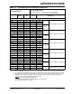
TABLE 21-2: THERMAL OPERATING CONDITIONS
Rating Symbol Min Typ Max Unit
dsPIC30F1010/202X-30I
Operating Junction Temperature Range T
J -40 +125 °C
Operating Ambient Temperature Range TA -40 +85 °C
dsPIC30F1010/202X-20E
Operating Junction Temperature Range T
J -40 +150 °C
Operating Ambient Temperature Range TA -40 +125 °C
Power Dissipation:
Internal chip power dissipation:
PD PINT + PI/O W
I/O Pin power dissipation:
Maximum Allowed Power Dissipation PDMAX (TJ - TA) / θJA W
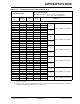
TABLE 21-3: THERMAL PACKAGING CHARACTERISTICS
Characteristic Symbol Typ Max Unit Notes
Package Thermal Resistance, 28-pin SOIC (SO) θJA 48.3 °C/W 1, 2
Package Thermal Resistance, 28-pin QFN θJA 33.7 °C/W 1, 2
Package Thermal Resistance, 28-pin SPDIP (SP) θJA 42 °C/W 1, 2
Package Thermal Resistance, 44-pin QFN
θJA 28 °C/W 1, 2
Package Thermal Resistance, 44-pin TQFP θJA 39.3 °C/W 1, 2
Note 1: Junction to ambient thermal resistance, Theta-ja (θJA) numbers are achieved by package simulations.
2: Depending on operating conditions, air flow may be required for improved thermal performance.
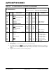
TABLE 21-4: DC TEMPERATURE AND VOLTAGE SPECIFICATIONS
DC CHARACTERISTICS
Standard Operating Conditions: 3.3V and 5.0V (±10%)
(unless otherwise stated)
Operating temperature -40°C ≤ TA ≤ +85°C for Industrial
-40°C ≤ T
A ≤ +125°C for Extended
Param
No.
Symbol Characteristic Min Typ
(1)
Max Units Conditions
Operating Voltage
(2)
DC10 VDD Supply Voltage 3.0 — 5.5 V Industrial temperature
DC11 VDD Supply Voltage 3.0 — 5.5 V Extended temperature
DC12 V
DR RAM Data Retention Voltage
(3)
—1.5—V
DC16 VPOR VDD Start Voltage
to ensure internal
Power-on Reset signal
—VSS —V
DC17 SVDD VDD Rise Rate
to ensure internal
Power-on Reset signal
0.05 V/ms 0-5V in 0.1 sec
0-3.3V in 60 ms
Note 1: Data in “Typ” column is at 5V, 25°C unless otherwise stated. Parameters are for design guidance only and
are not tested.
2: These parameters are characterized but not tested in manufacturing.
3: This is the limit to which V
DD can be lowered without losing RAM data.
P
INT
V
DD
I
DD
I
OH
∑
–()×=
P
I/O
V
DD
V
OH
–
{}
I
OH
×()
∑
V
OL
I
OL
×
()
∑
+=