
Datasheet


dsPIC30F1010/202X
DS70178C-page 218 Preliminary © 2006 Microchip Technology Inc.
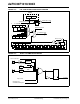
TABLE 18-8: SYSTEM INTEGRATION REGISTER MAP FOR dsPIC30F202X
SFR
Name
Addr
.
Bit 15 Bit 14 Bit 13 Bit 12 Bit 11 Bit 10 Bit 9 Bit 8 Bit 7 Bit 6 Bit 5 Bit 4 Bit 3 Bit 2 Bit 1 Bit 0 Reset State
RCON 0740 TRAPR IOPUWR — — — — — — EXTR SWR SWDTEN WDTO SLEEP IDLE — POR Depends on type of Reset.
OSCCON 0742
— COSC<2:0> — NOSC<2:0> CLKLOCK — LOCK PRCDEN CF TSEQEN — OSWEN Depends on Configuration bits.
OSCTUN
0748 TSEQ3<3:0> TSEQ2<3:0> TSEQ1<3:0> TUN<3:0>
0000 0000 0000 0000
OSCTUN2 074A TSEQ7<3:0> TSEQ6<3:0> TSEQ5<3:0> TSEQ4<3:0>
0000 0000 0000 0000
LFSR 074C — LFSR<14:0>
0000 0000 0000 0000
PMD1 0770 — —T3MDT2MDT1MD — PWMMD —I2CMD—U1MD — SPI1MD — —ADCMD
0000 0000 0000 0000
PMD2 0772 — — — — — — —IC1MD — — — — — —OC2MDOC1MD
0000 0000 0000 0000
PMD3
0774
— — — —
CMP_PSMD
— — — — — — — — — — —
0000 0000 0000 0000
Note: Refer to the “dsPIC30F Family Reference Manual” (DS70046) for descriptions of register bit fields.
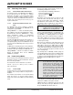
TABLE 18-9: DEVICE CONFIGURATION REGISTER MAP
File Name Addr. Bits 23-16 Bit 15 Bit 14 Bit 13 Bit 12 Bit 11 Bit 10 Bit 9 Bit 8 Bit 7 Bit 6 Bit 5 Bit 4 Bit 3 Bit 2 Bit 1 Bit 0
FBS F80000
— — — — — — — — — — — — — BSS<2:0> BWRP
FGS F80004
— — — — — — — — — — — — — — GSS1 GSS0 GWRP
FOSCSEL F80006
— — — — — — — — — — — — — — —FNOSC<1:0>
FOSC F80008
— — — — — — — — — FCKSM<1:0> FRANGE — —
OSCIOFNC
POSCMD<1:0>
FWDT F8000A
— — — — — — — — — FWDTEN WWDTEN —
WDTPRE
WDTPOST<3:0>
FPOR F8000C
— — — — — — — — — — — — — —FPWRT<2:0>
Note: Refer to the “dsPIC30F Family Reference Manual” (DS70046) for descriptions of register bit fields.