
Datasheet


© 2006 Microchip Technology Inc. Preliminary DS70178C-page 211
dsPIC30F1010/202X
18.7.1 POR: POWER-ON RESET
A power-on event will generate an internal POR pulse
when a V
DD rise is detected. The Reset pulse will occur
at the POR circuit threshold voltage (V
POR), which is
nominally 1.85V. The device supply voltage character-
istics must meet specified starting voltage and rise rate
requirements. The POR pulse will reset a POR timer
and place the device in the Reset state. The POR also
selects the device clock source identified by the
oscillator configuration fuses.
The POR circuit inserts a small delay, T
POR, which is
nominally 10 μs and ensures that the device bias
circuits are stable. Furthermore, a user selected power-
up time-out (T
PWRT) is applied. The TPWRT parameter
is based on Configuration bits and can be 0 ms (no
delay), 4 ms, 16 ms or 64 ms. The total delay is at
device power-up T
POR + TPWRT. When these delays
have expired, SYSRST
will be negated on the next
leading edge of the Q1 clock, and the PC will jump to
the Reset vector.
The timing for the SYSRST
signal is shown in
Figure 18-8 through Figure 18-10.
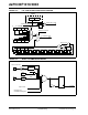
FIGURE 18-8: TIME-OUT SEQUENCE ON POWER-UP (MCLR TIED TO VDD)
FIGURE 18-9: TIME-OUT SEQUENCE ON POWER-UP (MCLR
NOT TIED TO VDD): CASE 1
TPWRT
TOST
VDD
Internal POR
PWRT Time-out
OST Time-out
Internal Reset
MCLR
TPWRT
TOST
VDD
Internal POR
PWRT Time-out
OST Time-out
Internal Reset
MCLR