
Datasheet


© 2006 Microchip Technology Inc. Preliminary DS70178C-page 207
dsPIC30F1010/202X
18.4 PRIMARY OSCILLATOR ON OSC1/
OSC2 PINS:
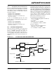
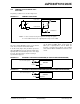
The primary oscillator uses is shown in Figure 18-3.
FIGURE 18-3: PRIMARY OSCILLATOR
18.5 EXTERNAL CLOCK INPUT
Two of the primary Oscillator modes use an external
clock. These modes are EC and EC with IO.
In the EC mode (Figure 18-4), the OSC1 pin can be
driven by CMOS drivers. In this mode, the OSC1 pin is
high-impedance and the OSC2 pin is the clock output
(F
OSC/2). This output clock is useful for testing or
synchronization purposes.
In the EC with IO mode (Figure 18-5), the OSC1 pin
can be driven by CMOS drivers. In this mode, the
OSC1 pin is high-impedance and the OSC2 pin
becomes a general purpose I/O pin. The feedback
device between OSC1 and OSC2 is turned off to save
current.
FIGURE 18-4: EXTERNAL CLOCK INPUT OPERATION (EC OSCILLATOR CONFIGURATION)
FIGURE 18-5: EXTERNAL CLOCK INPUT OPERATION (ECIO OSCILLATOR CONFIGURATION)
C1
C2
XTAL
OSC2/CLKO
Rs
(1)
OSC1/CLKI
RF
(2)
Note 1: A series resistor, Rs, may be required for AT strip cut crystals.
2: The feedback resistor, R
F, is typically in the range of 2 to 10 MΩ.
To CLKGE N
CLKO/RC15
OSC1
OSC2
F
OSC/2
dsPIC30F
Clock from Ext System
OSC1
I/O (OSC2)
I/O
dsPIC30F
Clock from Ext System