
Datasheet


dsPIC30F1010/202X
DS70178C-page 206 Preliminary © 2006 Microchip Technology Inc.
18.3.1 INITIAL CLOCK SOURCE
SELECTION
While coming out of a Power-on Reset, the device
selects its clock source based on:
a) FNOSC<1:0> Configuration bits that select one
of three oscillator groups (HS, EC or FRC)
b) POSCMD1<1:0> Configuration bits that select
the Primary Oscillator Mode
c) OSCIOFNC selects if the OSC2 pin is an I/O or
clock output
The selection is as shown in Table 18-1.
TABLE 18-1: CONFIGURATION BIT VALUES FOR CLOCK SELECTION
18.3.2 OSCILLATOR START-UP TIMER
(OST)
In order to ensure that a crystal oscillator (or ceramic
resonator) has started and stabilized, an Oscillator
Start-up Timer is included. It is a simple 10-bit counter
that counts 1024 T
OSC cycles before releasing the
oscillator clock to the rest of the system. The time-out
period is designated as T
OST. The TOST time is involved
every time the oscillator has to restart (i.e., on POR and
wake-up from Sleep). The Oscillator Start-up Timer is
applied to the HS Oscillator mode (upon
wake-up from Sleep and POR) for the primary
oscillator.
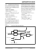
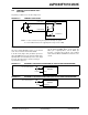
18.3.3 PHASE LOCKED LOOP (PLL)
The PLL multiplies the clock, which is generated by the
primary oscillator. The PLL is selectable to have a gain
of x32 only. Input and output frequency ranges are
summarized in Table 18-2.
TABLE 18-2: PLL FREQUENCY RANGE
The PLL features a lock output, which is asserted when
the PLL enters a phase locked state. Should the loop
fall out of lock (e.g., due to noise), the lock signal will be
rescinded. The state of this signal is reflected in the
read-only LOCK bit in the OSCCON register.
Oscillator
Mode
Oscillator
Source
FNOSC<1:0> POSCMD<1:0>
OSCIOFNC
OSC2
Function
OSC1
Function
Bit 1 Bit 0 Bit 1 Bit 0
HS w/PLL 32x PLL 11 1 0 N/A CLKO
(1)
CLKI
FRC w/PLL 32x PLL 01 1 1 1 CLKO I/O
FRC w/PLL 32x PLL 01 1 1 0 I/O I/O
EC w/PLL 32x PLL 11 0 0 1 CLKO CLKI
EC w/PLL 32x PLL 11 0 0 0 I/O CLKI
EC
(2)
External 100 0 1 CLKO CLKI
EC
(2)
External 100 0 0 I/O CLKI
HS
(2)
External 101 0 N/A CLKO
(1)
CLKI
FRC
(2)
Internal RC 00 1 1 0 I/O I/O
FRC
(2)
Internal RC 00 1 1 1 CLKO I/O
Note 1: CLKO is not recommended to drive external circuits.
2: This mode is not recommended for some applications; disabling 32x PLL will not allow operation of
high-speed ADC and PWM.
FIN
PLL
Multiplier
F
OUT
6.4 MHz x32 205 MHz
9.7 MHz x32 310 MHz
14.55 MHz x32 466 MHz